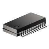
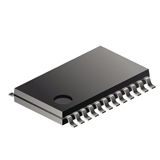
SN74LV166ADBR
8位并联负载移位寄存器 8-BIT PARALLEL-LOAD SHIFT REGISTERS
The "LV166A devices are 8-bit parallel-load shift registers, designed for 2-V to 5.5-V VCC operation.
The "LV166A parallel-in or serial-in, serial-out registers feature gated clock CLK, CLK INH inputs and an overriding clear CLR\\\\ input. The parallel-in or serial-in modes are established by the shift/load SH/LD\\\\ input. When high, SH/LD\ enables the serial SER data input and couples the eight flip-flops for serial shifting with each clock CLK pulse. When low, the parallel broadside data inputs are enabled, and synchronous loading occurs on the next clock pulse. During parallel loading, serial data flow is inhibited. Clocking is accomplished on the low-to-high-level edge of CLK through a 2-input positive-NOR gate, permitting one input to be used as a clock-enable or clock-inhibit function. Holding either CLK or CLK INH high inhibits clocking; holding either low enables the other clock input. This allows the system clock to be free running, and the register can be stopped on command with the other clock input. CLK INH should be changed to the high level only when CLK is high. CLR\ overrides all other inputs, including CLK, and resets all flip-flops to zero.
These devices are fully specified for partial-power-down applications using Ioff. The Ioff circuitry disables the outputs, preventing damaging current backflow through the devices when they are powered down.

