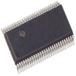
SN74ALVCH16835DGVR
18位通用总线驱动器,具有三态输出 18-BIT UNIVERSAL BUS DRIVER WITH 3-STATE OUTPUTS
This 18-bit universal bus driver is designed for 1.65-V to 3.6-V VCC operation.
Data flow from A to Y is controlled by the output-enable OE\ input. The device operates in the transparent mode when the latch-enable LE input is high. The A data is latched if the clock CLK input is held at a high or low logic level. If LE is low, the A data is stored in the latch/flip-flop on the low-to-high transition of CLK. When OE\ is high, the outputs are in the high-impedance state.
To ensure the high-impedance state during power up or power down, OE\ should be tied to VCC through a pullup resistor; the minimum value of the resistor is determined by the current-sinking capability of the driver.
Active bus-hold circuitry holds unused or undriven inputs at a valid logic state. Use of pullup or pulldown resistors with the bus-hold circuitry is not recommended.