CD4502BNSR
CMOS选通六反相器/缓冲器 CMOS Strobed Hex Inverter/Buffer
CD4502B consists of six inverter/buffers with 3-state outputs. A logic "1" on the OUTPUT DISABLE input produces a high-impedance state in all six outputs. This feature permits common busing of the outputs, thus simplifying system design. A Logic "1" on the INHIBIT input switches all six outputs to logic "0" if the OUTPUT DISABLE input is a logic "0". This device is capable of driving two standard TTL loads, which is equivalent to six times the JEDEC "B"-series IOL standard.
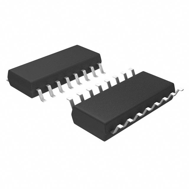
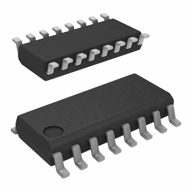
The CD4502B types are supplied in 16-lead hermetic dual-in-line ceramic packages F3A suffix, 16-lead dual-in-line plastic packages E suffix, 16-lead small-outline packages NSR suffix, and 16-lead thin shrink small-outline packages PW and PWR suffixes.