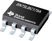
SN75LBC179A
低功耗差动线路驱动器和接收器对
The SN65LBC179A and differential driver and receiver pairs are monolithic integrated circuits designed for bidirectional data communication over long cables that take on the characteristics of transmission lines. They are balanced, or differential, voltage mode devices that are compatible with ANSI standard A/EIA-485-A and ISO 8482:1987E. The A version offers improved switching performance over its predecessors without sacrificing significantly more power.
The SN65LBC179A and SN75LBC179A combine a differential line driver and differential input line receiver and operate from a single 5-V supply. The driver differential outputs and the receiver differential inputs are connected to separate terminals for full-duplex operation and are designed to present minimum loading to the bus when powered off VCC = 0. These parts feature a wide positive and negative common-mode voltage range making them suitable for point-to-point or multipoint data bus applications. The devices also provide positive- and negative-current limiting and thermal shutdown for protection from line fault conditions.
The SN65LBC179A is characterized over the industrial temperature range of –40°C to 85°C. The SN75LBC179A is characterized for operation over the commercial temperature range of 0°C to 70°C.
- .
- High-Speed Low-Power LinBiCMOS Circuitry Designed
for Signaling Rates1 of up to 30 Mbps
- .
- Bus-Pin ESD Protection Exceeds 12 kV HBM
- .
- Very Low Disabled Supply-Current Requirements . . . 700 µA Max
- .
- Common-Mode Voltage Range of –7 V to 12 V
- .
- Low Supply Current . . .15 mA Max
- .
- Compatible With ANSI Standard TIA/EAI-485-A and ISO8482: 1987E
- .
- Positive and Negative Output Current Limiting
- .
- Driver Thermal Shutdown Protection
1Signaling rate by TIA/EIA-485-A definition restrict transition times to 30% of the bit length, and much higher signaling rates may be achieved without this requirement as displayed in the of this device.

