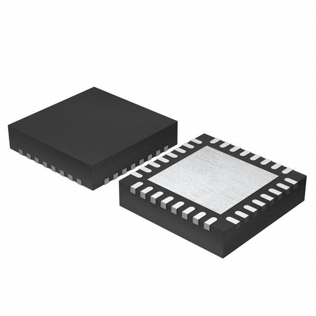
CDCU877BZQLT
时钟驱动器及分配 1.8v PLL Clock Driver
The CDCU877B is a high-performance, low-jitter, low-skew, zero-delay buffer that distributes a differential clock input pair CK, CK to ten differential pairs of clock outputs Yn, Yn and to one differential pair of feedback clock outputs FBOUT, FBOUT. The clock outputs are controlled by the input clocks CK, CK, the feedback clocks FBIN, FBIN, the LVCMOS control pins OE, OS, and the analog power input AVDD. When OE is low, the clock outputs, except FBOUT/FBOUT, are disabled while the internal PLL continues to maintain its locked-in frequency. OS output select is a program pin that must be tied to GND or VDD. When OS is high, OE functions as previously described. When OS and OE are both low, OE has no affect on Y7/Y7, they are free running. When AVDD is grounded, the PLL is turned off and bypassed for test purposes.
When both clock inputs CK, CK are logic low, the device enters in a low power mode. An input logic detection circuit on the differential inputs, independent from input buffers, detects the logic low level and performs in a low power state where all outputs, the feedback, and the PLL are off. When the clock inputs transition from being logic low to being differential signals, the PLL turns back on, the inputs and the outputs are enabled, and the PLL obtains phase lock between the feedback clock pair FBIN, FBIN and the clock input pair CK, CK within the specified stabilization time.
The CDCU877B is able to track spread spectrum clocking SSC for reduced EMI. This device operates from -40°C to 85°C.