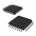
CDCLVP111MVFREP
时钟缓冲器 1:10 LVPECL Buffer w/ Selectable Input
The CDCLVP111 clock driver distributes one differential clock pair of LVPECL input, CLK0, CLK1 to ten pairs of differential LVPECL clock Q0, Q9 outputs with minimum skew for clock distribution. The CDCLVP111 can accept two clock sources into an input multiplexer. The CDCLVP111 is specifically designed for driving 50-Ω transmission lines. When an output pin is not used, leaving it open is recommended to reduce power consumption. If only one of the output pins from a differential pair is used, the other output pin must be identically terminated to 50 Ω.
The VBB reference voltage output is used if single-ended input operation is required. In this case, the VBB pin should be connected to CLK0 and bypassed to GND via a 10-nF capacitor.
However, for high-speed performance up to 3.5 GHz, the differential mode is strongly recommended.
The CDCLVP111 is characterized for operation from –55°C to 125°C.