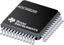
ADC08B200
具有捕捉缓冲器的 8 位、200 MSPS A/D 转换器
The is a high speed analog-to-digital converter ADC with an integrated capture buffer. The 8-bit, 200 MSPS A/D core is based upon the proven ADC08200 with integrated track-and-hold and is optimized for low power consumption. This device contains a selectable size capture buffer of up to 1,024 bytes that allows fast capture of an input signal with a slower readout rate. An on-chip clock PLL circuit provides the option of on-chip clock rate multiplication to provide the high speed sampling clock.
The ADC08B200 is resistant to latch-up and the outputs are short-circuit proof. The top and bottom of the ADC08B200"s reference ladder are available for connections, enabling a wide range of input possibilities. The digital outputs are TTL/CMOS compatible with a separate output power supply pin to support interfacing with 2.7V to 3.3V logic. The digital inputs and outputs are low voltage TTL/CMOS compatible and the output data format is straight binary.
The ADC08B200Q runs on an Automotive Grade Flow and is AEC-Q100 Grade 2 Qualified.
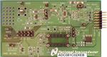
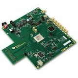
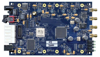
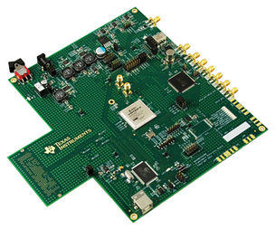
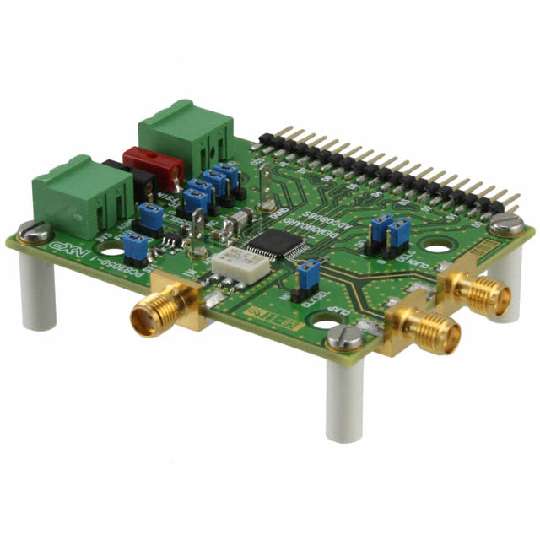
The ADC08B200 is offered in a 48-pin plastic package TQFP and is specified over the extended industrial temperature range of −40°C to +105°C. An evaluation board is available to assist in the easy evaluation of the ADC08B200.
- .
- Single-Ended Input
- .
- Selectable Capture Buffer Size
- .
- PLL for Clock Multiplication
- .
- Reference Ladder Top and Bottom Accessible
- .
- Linear Power Scaling with Sample Rate
- .
- FPGA Training Pattern
- .
- AEC-Q100 Grade 2 Qualified
- .
- Power-Down Feature
## Key Specifications
PLL Bypassed
- .
- Resolution 8 Bits
- .
- Maximum Sampling Frequency 200 MSPS min
- .
- DNL ±0.4 LSB typ
- .
- ENOB fIN= 49 MHz 7.2 bits typ
- .
- THD fIN= 49 MHz −53 dBc typ
- .
- Power Consumption
- .
- Operating 50 MHz Input 2 mW / Msps typ
- .
- Power Down 2.15 mW typ
All trademarks are the property of their respective owners.