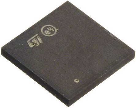
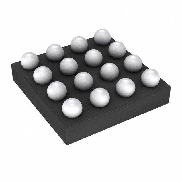
STHV748SQ
Quad +/- 90V, +/- 2A, 3/5 level, ESD-enhanced high-speed ultrasound pulser
This monolithic, high-voltage, high-speed pulser generator features four independent channels. It is designed for medical ultrasound imaging applications, but can also be used to drive piezoelectric, capacitive or MEMS based transducers.
The STHV748S is composed of a controller logic interface circuit, level translators, MOSFET gate drivers, noise blocking diodes, and high-power P-channel and N-channel MOSFETs as the output stage for each channel. It also includes clamping-to-ground circuitry, anti-leakage, anti-memory effect block, thermal sensor, and a T/R switch which guarantees effective decoupling during the transmission phase. The STHV748S also includes self-biasing and thermal shutdown blocks.
Each channel can support up to five active output levels with two half bridges. The output stage of each channel is able to provide ±2 A peak output current. In order to reduce power dissipation during continuous wave mode, a dedicated half-bridge is available and the peak current is limited to 0.6 A.
An ESD reinforced structure was developed to prevent high voltage overshoots and inrush current due to cabled transducer reflections. Each HV output is supported by a dedicate HV diode network to withstand possible reflections, mitigating excessive voltage overshoot that could lead to device damage.
**Key Features**
- .
- Pinout compatibility with STHV748
- .
- Recirculation current protection
- .
- 0 to ±90 V output voltage
- .
- Up to 20 MHz operating frequency
- .
- Embedded low-power, floating high-voltage drivers external voltage rails can be also used
- .
- Mode operations:
- .
- 3/5-level output waveform
- .
- ±2 A source and sink current
- .
- Down to ≤ 20 ps jitter
- .
- Anti-cross conduction function
- .
- Low 2nd harmonic distortion
- .
- Fully integrated clamping-to-ground function
- .
- 8 Ω synchronous active clamp
- .
- Anti-leakage on output node
- .
- Dedicated half bridge for continuous wave CW operations
- .
- ≤ 0.1 W power consumption
- .
- ±0.6 A source and sink current
- .
- 205 fs RMS jitter [100 Hz-20 kHz]
- .
- Fully integrated T/R switch
- .
- 13.5 Ω on-resistance
- .
- HV MOS topology to minimize current consumption
- .
- Up to 300 MHz BW
- .
- Receiver multiplexing function
- .
- 1.8 V to 3.6 V CMOS logic interface
- .
- New digital input compatibility @ 1.8 V
- .
- Auxiliary integrated circuits
- .
- Noise blocking diodes
- .
- Fully self-biasing architecture
- .
- Anti-memory effect for all internal HV nodes
- .
- Thermal protection
- .
- Standby function
- .
- Reinforced diodes on HV outputs for protection by recirculation current
- .
- Latch-up free due to HV SOI technology
- .
- Very few external passive components needed