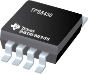
TPS5450
5.5V 至 36V 输入、5A、500kHz 降压转换器
The is a high-output-current PWM converter that integrates a low-resistance, high-side N-channel MOSFET. Included on the substrate with the listed features are a high-performance voltage error amplifier that provides tight voltage regulation accuracy under transient conditions; an undervoltage-lockout circuit to prevent start-up until the input voltage reaches 5.5 V; an internally set slow-start circuit to limit inrush currents; and a voltage feed-forward circuit to improve the transient response. Using the ENA pin, shutdown supply current is reduced to 18 μA typically. Other features include an active-high enable, overcurrent limiting, overvoltage protection and thermal shutdown. To reduce design complexity and external component count, the TPS5450 feedback loop is internally compensated.
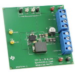
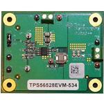
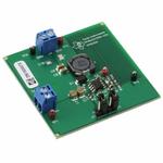
The TPS5450 device is available in a thermally-enhanced, 8-pin SOIC PowerPAD package. provides evaluation modules and software tool to aid in achieving high-performance power supply designs to meet aggressive equipment development cycles.
- .
- Wide Input Voltage Range: 5.5 V to 36 V
- .
- Up to 5-A Continuous 6-A Peak Output Current
- .
- High Efficiency Greater Than 90% Enabled by 110-mΩ
Integrated MOSFET Switch
- .
- Wide Output Voltage Range: Adjustable Down to 1.22 V
With 1.5% Initial Accuracy
- .
- Internal Compensation Minimizes External Part Count
- .
- Fixed 500-kHz Switching Frequency for Small Filter Size
- .
- 18-µA Shutdown Supply Current
- .
- Improved Line Regulation and Transient Response by Input
Voltage Feed Forward
- .
- System Protected by Overcurrent Limiting, Overvoltage
Protection and Thermal Shutdown
- .
- 40°C to 125°C Operating Junction
Temperature Range
- .
- Available in Small Thermally Enhanced 8-Pin SOIC PowerPAD™
Package