MX25L12845E
128M-BIT [x 1/x 2/x 4] CMOS MXSMIO® SERIAL MULTI I/O FLASH MEMORY
GENERAL DESCRIPTION
is 134,217,728 bits serial Flash memory, which is confgured as 16,777,216 x 8 internally. When it is in two or four I/O mode, the structure becomes 67,108,864 bits x 2 or 33,554,432 bits x 4. The MX25L12845E features a serial peripheral interface and software protocol allowing operation on a simple 3-wire bus. The three bus signals are a clock input SCLK, a serial data input SI, and a serial data output SO. Serial access to the device is enabled by CS# input.
MX25L12845E provides high performance read mode, which may latch address and data on both rising and falling edge of clock. By using this high performance read mode, the data throughput may be doubling. Moreover, the performance may reach direct code execution, the RAM size of the system may be reduced and further saving system cost.
MX25L12845E, MXSMIO Serial Multi I/O flash memory, provides sequential read operation on the whole chip and multi-I/O features.
FEATURES
GENERAL
• Serial Peripheral Interface compatible -- Mode 0 and Mode 3
• 128Mb: 134,217,728 x 1 bit structure or 67,108,864 x 2 bits two I/O mode structure or 33,554,432 x 4 bits four I/O mode structure
• 4096 Equal Sectors with 4K bytes each
- Any Sector can be erased individually
• 512 Equal Blocks with 32K bytes each
- Any Block can be erased individually
• 256 Equal Blocks with 64K bytes each
- Any Block can be erased individually
• Power Supply Operation
- 2.7 to 3.6 volt for read, erase, and program operations
• Latch-up protected to 100mA from -1V to Vcc +1V
PERFORMANCE
• High Performance
VCC = 2.7~3.6V
- Normal read
- 50MHz
- Fast read Normal Serial Mode
- 1 I/O: 104MHz with 8 dummy cycles
- 2 I/O: 70MHz with 4 dummy cycles
- 4 I/O: 70MHz with 6 dummy cycles
- Fast read Double Transfer Rate Mode
- 1 I/O: 50MHz with 6 dummy cycles
- 2 I/O: 50MHz with 6 dummy cycles
- 4 I/O: 50MHz with 8 dummy cycles
- Fast program time: 1.4mstyp. and 5msmax./page 256-byte per page
- Byte program time: 9us typical
- Continuously Program mode automatically increase address under word program mode
- Fast erase time: 60ms typ./sector 4K-byte per sector ; 0.7styp. /block 64K-byte per block; 80styp. /chip
• Low Power Consumption
- Low active read current: 19mAmax. at 104MHz, 15mAmax. at 66MHz and 10mAmax. at 33MHz
- Low active programming current: 25mA max.
- Low active erase current: 25mA max.
- Low standby current: 100uA max.
- Deep power down current: 40uA max.
• Typical 100,000 erase/program cycles
SOFTWARE FEATURES
• Input Data Format
- 1-byte Command code
• Advanced Security Features
- BP0-BP3 block group protect
- Flexible individual block protect when OTP WPSEL=1
- Additional 4K bits secured OTP for unique identifer
• Auto Erase and Auto Program Algorithms
- Automatically erases and verifes data at selected sector
- Automatically programs and verifes data at selected page by an internal algorithm that automatically times the program pulse width Any page to be programed should have page in the erased state frst.
• Status Register Feature
• Electronic Identifcation
- JEDEC 1-byte Manufacturer ID and 2-byte Device ID
- RES command for 1-byte Device ID
- REMS, REMS2, REMS4 and REMS4D commands for 1-byte Manufacturer ID and 1-byte Device ID
• Support Serial Flash Discoverable Parameters SFDP mode
HARDWARE FEATURES
• SCLK Input
- Serial clock input
• SI/SIO0
- Serial Data Input or Serial Data Input/Output for 2 x I/O mode and 4 x I/O mode
• SO/SIO1/PO7
- Serial Data Output or Serial Data Input/Output for 2 x I/O mode and 4 x I/O mode or Parallel Data
• WP#/SIO2
- Hardware write protection or serial data Input/Output for 4 x I/O mode
• NC/SIO3
- NC pin or serial data Input/Output for 4 x I/O mode
• PO0~PO6
- For parallel mode data only 128Mb provide parallel mode
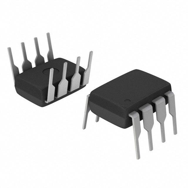
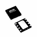
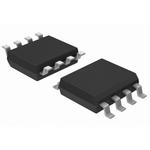
• PACKAGE
- 16-pin SOP 300mil
- 8-WSON 8x6mm
- All devices are RoHS Compliant and Halogen-free