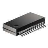
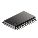
SN74AVC16646DGVR
16位总线收发器和寄存器具有三态输出 16-BIT BUS TRANSCEIVER AND REGISTER WITH 3-STATE OUTPUTS
A Dynamic Output Control DOC circuit is implemented, which, during the transition, initially lowers the output impedance to effectively drive the load and, subsequently, raises the impedance to reduce noise. Figure 1 shows typical VOL vs IOL and VOH vs IOH curves to illustrate the output impedance and drive capability of the circuit. At the beginning of the signal transition, the DOC circuit provides a maximum dynamic drive that is equivalent to a high-drive standard-output device. For more information, refer to the application reports, _AVC Logic Family Technology and Applications_, literature number SCEA006, and _Dynamic Output Control DOC_- .
- *__**TM_ Circuitry Technology and Applications_, literature number SCEA009.
This 16-bit bus transceiver and register is operational at 1.2-V to 3.6-V VCC, but is designed specifically for 1.65-V to 3.6-V VCC operation.
The SN74AVC16646 can be used as two 8-bit transceivers or one 16-bit transceiver. Data on the A or B bus is clocked into the registers on the low-to-high transition of the appropriate clock CLKAB or CLKBA input. Figure 2 illustrates the four fundamental bus-management functions that can be performed with the SN74AVC16646.
Output-enable OE\\\\ and direction-control DIR inputs are provided to control the transceiver functions. In the transceiver mode, data present at the high-impedance port may be stored in either register or in both. The select-control SAB and SBA inputs can multiplex stored and real-time transparent mode data.
The circuitry used for select control eliminates the typical decoding glitch that occurs in a multiplexer during the transition between stored and real-time data. DIR determines which bus receives data when OE\ is low. In the isolation mode OE\ high, A data may be stored in one register and/or B data may be stored in the other register.
When an output function is disabled, the input function is still enabled and may be used to store and transmit data. Only one of the two buses, A or B, can be driven at a time.
To ensure the high-impedance state during power up or power down, OE\ should be tied to VCC through a pullup resistor; the minimum value of the resistor is determined by the current-sinking capability of the driver.
This device is fully specified for partial-power-down applications using Ioff. The Ioff circuitry disables the outputs, preventing damaging current backflow through the device when it is powered down.
The SN74AVC16646 is characterized for operation from -40°C to 85°C. View datasheet View product folder

