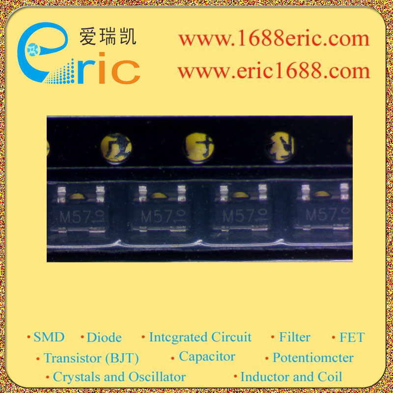
BF1100R
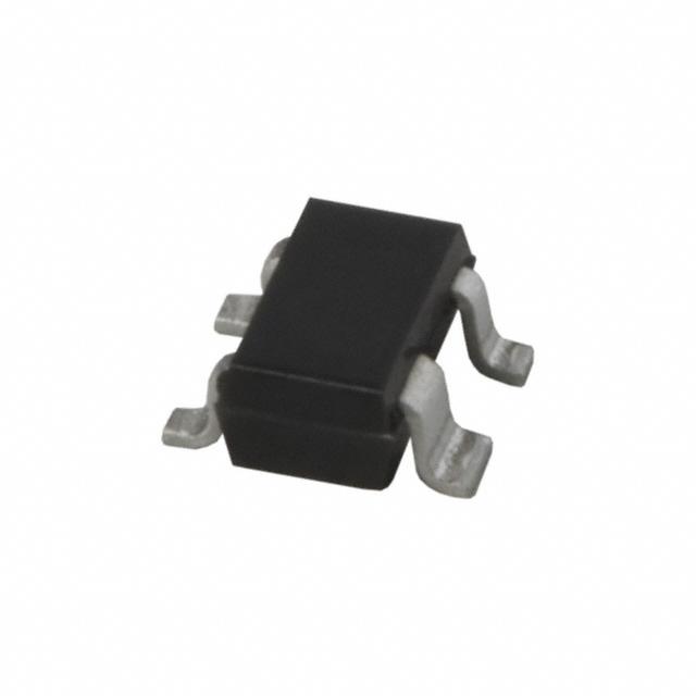
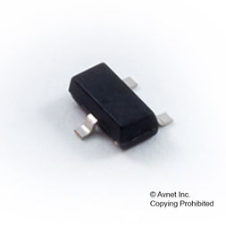
BF1100R N沟道MOSFET 14 30mA SOT-143 marking/标记 M57 高速开关/低导通电阻
最大源漏极电压Vds Drain-Source Voltage| 14V \---|--- 最大栅源极电压Vgs± Gate-Source Voltage| 13.2V 最大漏极电流Id Drain Current| 30mA 源漏极导通电阻ΩRds DΩ/Ohmain-SouΩ/Ohmce On-State Ω/Ohmesistance| 开启电压Vgs(th) Gate-Source Threshold Voltage| 0.3~1V 耗散功率Pd Power Dissipation| 200mW/0.2W Description & Applications| Dual-gate MOS-FETs FEATURES • Specially designed for use at 9 to 12 V supply voltage • Short channel transistor with high forward transfer admittance to input capacitance ratio • Low noise gain controlled amplifier up to 1 GHz • Superior cross-modulation performance during AGC. APPLICATIONS • VHF and UHF applications such as television tuners and professional communications equipment. DESCRIPTION Enhancement type field-effect transistor in a plastic microminiature SOT143 or SOT143R package. The transistor consists of an amplifier MOS-FET with source and substrate interconnected and an internal bias circuit to ensure good cross-modulation performance during AGC. 描述与应用| 双栅MOS场效应管 特点 •专为使用在9至12 V电源电压 •短沟道晶体管输入电容比具有较高的正向传输导纳 •低噪声增益控制放大器高达1 GHz •高级交叉调制性能在AGC。 应用 •VHF和UHF应用,如电视调谐器和专业的通信设备。 说明 增强型场效应晶体管在一个塑料的超小型SOT143或SOT143R包。该晶体管由MOS-FET源极和衬底的相互联系和内部偏置电路,以确保良好的交叉调制性能在AGC放大器。