THS4513
宽带、低噪声、低失真、全差动放大器
The is a wideband, fully-differential op amp designed for 3.3-V to 5-V data acquisition systems. It has very low noise at 2.2 nV/√Hz, and extremely low harmonic distortion of –75 dBc HD2 and –86 dBc HD3 at 70 MHz with 2-VPP output, G = 0 dB, and 200- load. Slew rate is very high at 5100 V/μs and with settling time of 2.9 ns to 1% 2-V step, it is ideal for pulsed applications. It is designed for a minimum gain of 0 dB.
To allow for dc-coupling to analog-to-digital converters ADCs, its unique output common-mode control circuit maintains the output common-mode voltage within 5-mV offset typ from the set voltage, when set within 0.5 V of midsupply, with less than 4-mV differential offset voltage. The common-mode set point is set to midsupply by internal circuitry, which may be overdriven from an external source.
The input and output are optimized for best performance with their common-mode voltages set to midsupply. Along with high performance at low power-supply voltage, this design makes it ideal for extremely high-performance, single-supply 5-V data acquisition systems.
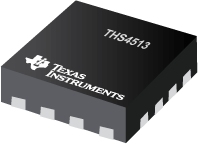
The THS4513 is offered in a quad, leadless QFN-16 package RGT, and is characterized for operation over the full industrial temperature range from –40°C to +85°C.
- .
- Fully-Differential Architecture
- .
- Centered Input Common-Mode Range
- .
- Minimum Gain of 1 V/V 0 dB
- .
- Bandwidth: 1600 MHz
- .
- Slew Rate: 5100 V/µs
- .
- 1% Settling Time: 2.9 ns
- .
- HD2: –75 dBc at 70 MHz
- .
- HD3: –86 dBc at 70 MHz
- .
- OIP2: 77 dBm at 70 MHz
- .
- OIP3: 42 dBm at 70 MHz
- .
- Input Voltage Noise: 2.2 nV/√Hz f > 10 MHz
- .
- Noise Figure: 19.8 dB
- .
- Output Common-Mode Control
- .
- Power Supply:
- .
- Voltage: 3 V ±1.5 V to 5 V ±2.5 V
- .
- Current: 37.7 mA
- .
- Power-Down Capability: 0.65 mA
- .
- APPLICA ONS
- .
- 5-V Data Acquisition Systems, High Linearity ADC Amplifier
- .
- Wireless Communication
- .
- Medical Imaging
- .
- Test and Measurement
All trademarks are the property of their respective owners.

