HD74ALVC1G80VSE
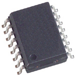
IC 上升沿触发器 HD74ALVC1G80VSE SOT-553/VSON-5 marking/标记 AC5
逻辑类型Logic Type| 设置(预设)和复位 SetPreset and Reset \---|--- 电路数Number of Circuits| D型 D-Type 输入数Number of Inputs| 差分 Differential 电源电压VccVoltage - Supply| 1 静态电流IqCurrent - Quiescent Max| 1 输出高,低电平电流Current - Output High, Low| 200MHz 低逻辑电平Logic Level - Low| 7.3nS 高逻辑电平Logic Level - High| 正边沿 Positive Edge 传播延迟时间@Vcc,CLMax Propagation Delay @ V, Max CL| 24mA,24mA Description & Applications| 0.5-4.6V 描述与应用| Single Positive Edge-triggered D-type Flip Flop Description The HD74ALVC1G80 has D-type flip flop in a 5 pin package. The input data is transferred to the output at the rising edge of clock pulse CLK. Low voltage and high-speed operation is suitable for the battery powered products e.g., notebook computers, and the low power consumption extends the battery life. Features • The basic gate function is lined up as Renesas uni logic series. • Supplied on emboss taping for high-speed automatic mounting. • Supply voltage range : 1.2 to 3.6 V Operating temperature range : −40 to +85°C • All inputs VIH Max. = 3.6 V @VCC = 0 V to 3.6 V All outputs VO Max. = 3.6 V @VCC = 0 V • Output current ±2 mA @VCC = 1.2 V ±4 mA @VCC = 1.4 V to 1.6 V ±6 mA @VCC = 1.65 V to 1.95 V ±18 mA @VCC = 2.3 V to 2.7 V ±24 mA @VCC = 3.0 V to 3.6 V

