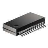
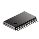
SN74LV367ANSR
HEX缓冲器和线路驱动器,具有三态输出 HEX BUFFERS AND LINE DRIVERS WITH 3-STATE OUTPUTS
The "LV367A devices are hex buffers and line drivers designed for 2-V to 5.5-V VCC operation. These devices are designed specifically to improve both the performance and density of 3-state memory address drivers, clock drivers, and bus-oriented receivers and transmitters.
The "LV367A devices are organized as dual 4-line and 2-line buffers/drivers with active-low output-enable 1OE\ and 2OE\\\\ inputs. When OE\ is low, the device passes noninverted data from the A inputs to the Y outputs. When OE\ is high, the outputs are in the high-impedance state.
To ensure the high-impedance state during power up or power down, OE\ should be tied to VCC through a pullup resistor; the minimum value of the resistor is determined by the current-sinking capability of the driver.

