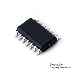
TLC274CNSR
该TLC274和TLC279四通道运算放大器结合了宽范围的输入失调电压等级的低失调电压漂移,高... The TLC274 and TLC279 quad operational amplifiers combine a wide range of input offset voltage grades with low offset voltage drift, high...
description
The TLC274 and TLC279 quad operational amplifiers combine a wide range of input offset voltage grades with low offset voltage drift, high input impedance, low noise, and speeds approaching that of general-purpose BiFET devices.
Trimmed Offset Voltage:
TLC279. . . 900 µV Max at 25°C, VDD= 5 V
Input Offset Voltage Drift...Typicall 0.1 µV/Month, Including the First 30 Days
Wide Range of Supply Voltages Over Specified Temperature Range:
0°C to 70°C...3 V to 16 V
−40°C to 85°C...4 V to 16 V
−55°C to 125°C...4 V to 16 V
Single-Supply Operation
Common-Mode Input Voltage Range Extends Below the Negative Rail C-Suffix and I-Suffix Versions
Low Noise...Typically 25 nV/√Hz at f = 1 kHz
Output Voltage Range Includes Negative Rail
High Input Impedance...1012ΩTyp
ESD-Protection Circuitry
Small-Outline Package Option Also Available in Tape and Reel
Designed-In Latch-Up Immunity