TMS320C5515
定点数字信号处理器
The device is a member of "s TMS320C5000™ fixed-point Digital Signal Processor DSP product family and is designed for low-power applications.
The fixed-point DSP is based on the TMS320C55x™ DSP generation CPU processor core. The C55x™ DSP architecture achieves high performance and low power through increased parallelism and total focus on power savings. The CPU supports an internal bus structure that is composed of one program bus, one 32-bit data read bus and two 16-bit data read buses, two 16-bit data write buses, and additional buses dedicated to peripheral and DMA activity. These buses provide the ability to perform up to four 16-bit data reads and two 16-bit data writes in a single cycle. The device also includes four DMA controllers, each with 4 channels, providing data movement for 16-independent channel contexts without CPU intervention. Each DMA controller can perform one 32-bit data transfer per cycle, in parallel and independent of the CPU activity.
The C55x CPU provides two multiply-accumulate MAC units, each capable of 17-bit x 17-bit multiplication and a 32-bit add in a single cycle. A central 40-bit arithmetic/logic unit ALU is supported by an additional 16-bit ALU. Use of the ALUs is under instruction set control, providing the ability to optimize parallel activity and power consumption. These resources are managed in the Address Unit AU and Data Unit DU of the C55x CPU.
The C55x CPU supports a variable byte width instruction set for improved code density. The Instruction Unit IU performs 32-bit program fetches from internal or external memory and queues instructions for the Program Unit PU. The Program Unit decodes the instructions, directs tasks to the Address Unit AU and Data Unit DU resources, and manages the fully protected pipeline. Predictive branching capability avoids pipeline flushes on execution of conditional instructions.
The general-purpose input and output functions along with the 10-bit SAR ADC provide sufficient pins for status, interrupts, and bit I/O for LCD displays, keyboards, and media interfaces. Serial media is supported through two MultiMedia Card/Secure Digital MMC/SD peripherals, four Inter-IC Sound I2S Bus™ modules, one Serial-Port Interface SPI with up to 4 chip selects, one I2C multi-master and slave interface, and a Universal Asynchronous Receiver/Transmitter UART interface.
The device peripheral set includes an external memory interface EMIF that provides glueless access to asynchronous memories like EPROM, NOR, NAND, and SRAM, as well as to high-speed, high-density memories such as synchronous DRAM SDRAM and mobile SDRAM mSDRAM. Additional peripherals include: a high-speed Universal Serial Bus USB2.0 device mode only, and a real-time clock RTC. This device also includes three general-purpose timers with one configurable as a watchdog timer, and an analog phase-locked loop APLL clock generator.
In addition, the device includes a tightly-coupled FFT Hardware Accelerator. The tightly-coupled FFT Hardware Accelerator supports 8 to 1024-point in power of 2 real and complex-valued FFTs.
Furthermore, the device includes three integrated LDOs DSP_LDO, ANA_LDO, and USB_LDO to power different sections of the device. The DSP_LDO can provide 1.3 V or 1.05 V to the DSP core CVDD, selectable on-the-fly by software as long as operating frequency ranges are observed. To allow for lowest power operation, the programmer can shutdown the internal DSP_LDO cutting power to the DSP core CVDD while an external supply provides power to the RTC CVDDRTC and DVDDRTC. The ANA_LDO is designed to provide 1.3 V to the DSP PLL VDDA_PLL, SAR, and power management circuits VDDA_ANA. The USB_LDO provides 1.3 V to USB core digital USB_VDD1P3 and PHY circuits USB_VDDA1P3. The RTC alarm interrupt or the WAKEUP pin can re-enable the internal DSP_LDO and re-apply power to the DSP core.
The device is supported by the industry’s award-winning eXpressDSP™, Code Composer Studio™ Integrated Development Environment IDE, DSP/BIOS™, Texas Instruments’ algorithm standard, and the industry’s largest third-party network. Code Composer Studio IDE features code generation tools including a C Compiler and Linker, RTDX™, XDS100™, XDS510™, XDS560™ emulation device drivers, and evaluation modules. The device is also supported by the C55x DSP Library which features more than 50 foundational software kernels FIR filters, IIR filters, FFTs, and various math functions as well as chip support libraries.
- .
- High-Performance, Low-Power, TMS320C55x™ Fixed-Point Digital Signal Processor
- .
- 16.67-, 13.33-, 10-, 8.33-ns Instruction Cycle Time
- .
- 60-, 75-, 100-, 120-MHz Clock Rate
- .
- One/Two Instructions Executed per Cycle
- .
- Dual Multipliers [Up to 200 or 240 Million Multiply-Accumulates per Second MMACS]
- .
- Two Arithmetic/Logic Units ALUs
- .
- Three Internal Data/Operand Read Buses and Two Internal Data/Operand Write Buses
- .
- Software-Compatible With C55x Devices
- .
- Industrial Temperature Devices Available
- .
- 320K Bytes Zero-Wait State On-Chip RAM, Composed of:
- .
- 64K Bytes of Dual-Access RAM DARAM, 8 Blocks of 4K x 16-Bit
- .
- 256K Bytes of Single-Access RAM SARAM, 32 Blocks of 4K x 16-Bit
- .
- 128K Bytes of Zero Wait-State On-Chip ROM
4 Blocks of 16K x 16-Bit
- .
- 4M x 16-Bit Maximum Addressable External Memory Space SDRAM/mSDRAM
- .
- 16-/8-Bit External Memory Interface EMIF with Glueless Interface to:
- .
- 8-/16-Bit NAND Flash, 1- and 4-Bit ECC
- .
- 8-/16-Bit NOR Flash
- .
- Asynchronous Static RAM SRAM
- .
- SDRAM/mSDRAM 1.8-, 2.5-, 2.75-, and 3.3-V
- .
- Direct Memory Access DMA Controller
- .
- Four DMA With 4 Channels Each 16-Channels Total
- .
- Three 32-Bit General-Purpose Timers
- .
- One Selectable as a Watchdog and/or GP
- .
- Two MultiMedia Card/Secure Digital MMC/SD Interfaces
- .
- Universal Asynchronous Receiver/Transmitter UART
- .
- Serial-Port Interface SPI With Four Chip-Selects
- .
- Master/Slave Inter-Integrated Circuit I2C Bus™
- .
- Four Inter-IC Sound I2S Bus™ for Data Transport
- .
- Device USB Port With Integrated 2.0 High-Speed PHY that Supports:
- .
- USB 2.0 Full- and High-Speed Device
- .
- LCD Bridge With Asynchronous Interface
- .
- Tightly-Coupled FFT Hardware Accelerator
- .
- 10-Bit 4-Input Successive Approximation SAR ADC
- .
- Real-Time Clock RTC With Crystal Input, With Separate Clock Domain and Power Supply
- .
- Four Core Isolated Power Supply Domains: Analog, RTC, CPU and Peripherals, and USB
- .
- Four I/O Isolated Power Supply Domains: RTC I/O, EMIF I/O, USB PHY, and DVDDIO
- .
- Three integrated LDOs DSP_LDO, ANA_LDO, and USB_LDO to power the isolated domains: DSP Core, Analog, and USB Core, respectively
- .
- Low-Power S/W Programmable Phase-Locked Loop PLL Clock Generator
- .
- On-Chip ROM Bootloader RBL to Boot From NAND Flash, NOR Flash, SPI EEPROM, SPI Serial Flash or I2C EEPROM
- .
- IEEE-1149.1 JTAG
Boundary-Scan-Compatible
- .
- Up to 26 General-Purpose I/O GPIO Pins
Multiplexed With Other Device Functions
- .
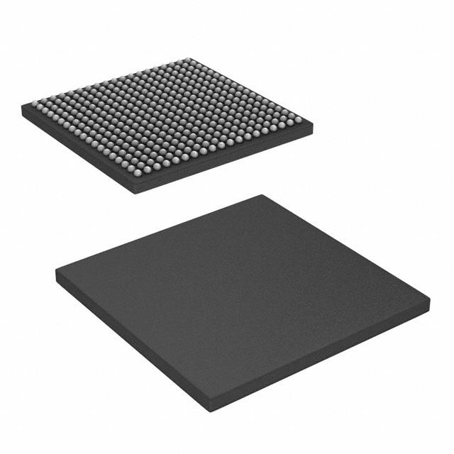
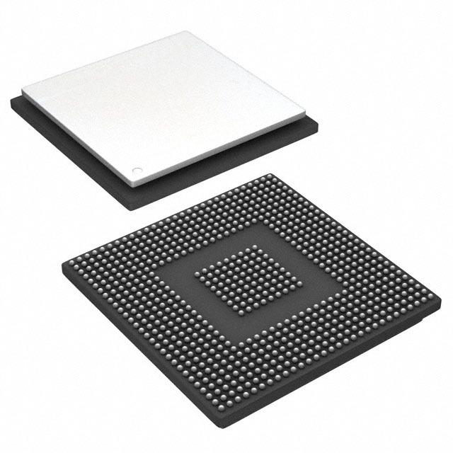
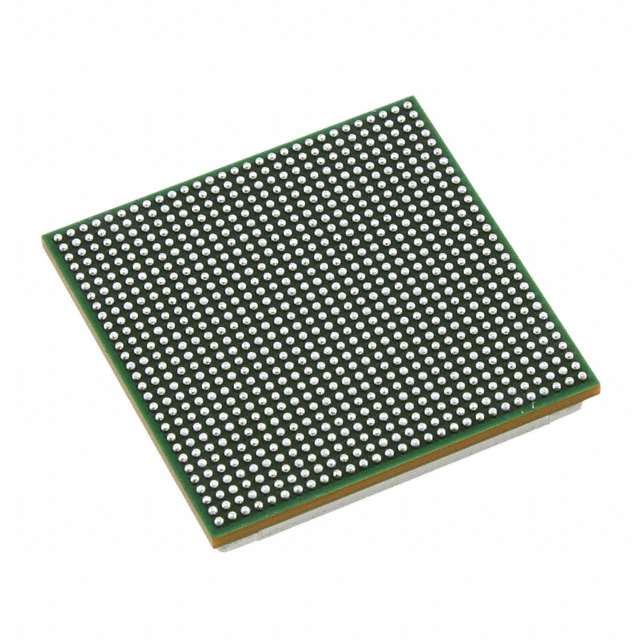
- 196-Terminal Pb-Free Plastic BGA Ball Grid Array ZCH Suffix
- .
- 1.05-V Core 60 or 75 MHz, 1.8-V, 2.5-V, 2.75-V, or 3.3-V I/Os
- .
- 1.3-V Core 100, 120 MHz, 1.8-V, 2.5-V, 2.75-V, or 3.3-V I/Os
All trademarks are the property of their respective owners. All trademarks are the property of their respective owners.