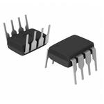
LTC1151CN8#PBF
LINEAR TECHNOLOGY LTC1151CN8#PBF 运算放大器, 双路, 2 MHz, 2个放大器, 2.5 V/µs, 4.75V 至 36V, DIP, 8 引脚
The is a high voltage/performance dual zero-drift Operational Amplifier for use with electronic scales. The two sample-and-hold capacitors per amplifier required externally by other chopper amplifiers are integrated on-chip. The LTC1151 also incorporates proprietary high voltage CMOS structures which allow operation at up to 36V total supply voltage. The LTC1151 has a typical offset voltage of 0.5µV, drift of 0.01µV/°C, 0.1 to 10Hz input noise voltage of 1.5µVP-P and a typical voltage gain of 140dB. It has a slew rate of 3V/µs and a gain-bandwidth product of 2.5MHz with a supply current of 0.9mA per amplifier. Overload recovery times from positive and negative saturation are 3 and 20ms, respectively.
- .
- ±18V High voltage operation
- .
- No external components required
- .
- 5µV Maximum offset voltage
- .
- 106dB Minimum CMRR
- .
- 110dB Minimum PSRR
- .
- Input common mode range includes ground