V62/06659-01XE
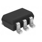
双缓冲门 DUAL BUFFER GATE
DESCRIPON/ORDERING INFORMATION
The SN74LVC2G34 is a dual buffer gate designed for 1.65-V to 5.5-V VCC operation. The SN74LVC2G34 performs the Boolean function Y = A in positive logic.
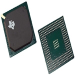
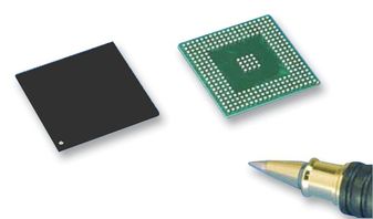
NanoStar™ and NanoFree™ package technology is a major breakthrough in IC packaging concepts, using the die as the package.
This device is fully specified for partial-power-down applications using Ioff. The Ioff circuitry disables the outputs, preventing damaging current backflow through the device when it is powered down.
FEATURES
• Controlled Baseline
– One Assembly Site
– One Test Site
– One Fabrication Site
• Extended Temperature Performance of –55°C to 125°C
• Enhanced Diminishing Manufacturing Sources DMS Support
• Enhanced Product-Change Notification
• QualificationPedigree 1
• Supports 5-V VCC Operation
• Inputs Accept Voltages to 5.5 V
• Max tpd of 4.1 ns at 3.3 V
• Low-Power Consumption, 10-µA Max ICC
• ±24-mA Output Drive at 3.3 V
• Typical VOLP Output Ground Bounce
<0.8 V at VCC = 3.3 V, TA = 25°C
• Typical VOHV Output VOH Undershoot
>2 V at VCC = 3.3 V, TA = 25°C
• Ioff Supports Partial-Power-Down Mode Operation
• Latch-Up Performance Exceeds 100 mA Per JESD 78, Class II
• ESD Protection Exceeds JESD 22
– 2000-V Human-Body Model A114-A
– 200-V Machine Model A115-A
– 1000-V Charged-Device Model C101