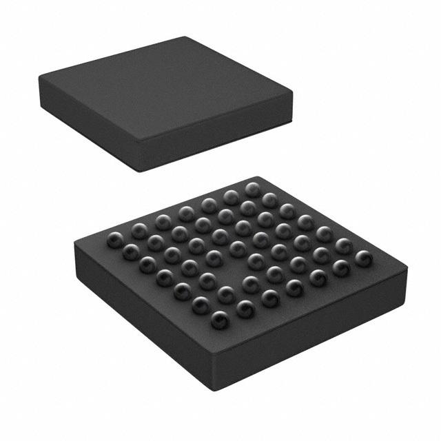
SN65LVDS307ZQCR
可编程27位并行到串行发送器 PROGRAMMABLE 27-BIT PARALLEL-TO-SERIAL TRANSMITTER
The SN65LVDS307 serializer device converts 27 parallel data inputs to one or two sub-low-voltage differential signaling SubLVDS serial outputs. It loads a shift register with 24 pixel bits and 3 control bits from the parallel CMOS input interface. In addition to the 27 data bits, the device adds a parity bit and two reserved bits into a 30-bit data word. Each word is latched into the device by the pixel clock PCLK. The parity bit odd parity allows a receiver to detect single bit errors. The serial shift register is uploaded at 30 or 15 times the pixel-clock data rate, depending on the number of serial links used. A copy of the pixel clock is output on a separate differential output.
FPC cabling typically interconnects the SN65LVDS307 with the display. Compared to parallel signaling, the SN65LVDS307 outputs significantly reduce the EMI of the interconnect by over 20 dB.
The SN65LVDS307 supports three power modes shutdown, standby, and active to conserve power. When transmitting, the PLL locks to the incoming pixel clock, PCLK, and generates an internal high-speed clock at the line rate of the data lines. The parallel data are latched on the rising or falling edge of PCLK, as selected by the external control signal CPOL. The serialized data is presented on the serial outputs D0 and D1, together with a recreated PCLK that is generated from the internal high-speed clock and output on CLK. If PCLK stops, the device enters a standby mode to conserve power.
The link select line, LS, controls whether one or two serial links are used. The TXEN input may be used to put the SN65LVDS307 in a shutdown mode. The SN65LVDS307 enters an active standby mode if the input clock, PCLK, stops. This minimizes power consumption without the need for controlling an external terminal. The SN65LVDS307 is characterized for operation over ambient air temperatures of -40°C to 85°C. All CMOS inputs offer failsafe to protect the input from damage during power up and to avoid current flow into the device inputs during power up. An input voltage of up to 2.165 V can be applied to all CMOS inputs while VDD is between 0 V and 1.65 V.