AD5313RBCPZ-RL7
双通道, 10位属于nanoDAC与2 PPM /℃参考, SPI接口 Dual, 10-Bit nanoDAC with 2 ppm/C Reference, SPI Interface
Product Details
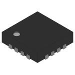
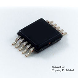
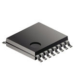
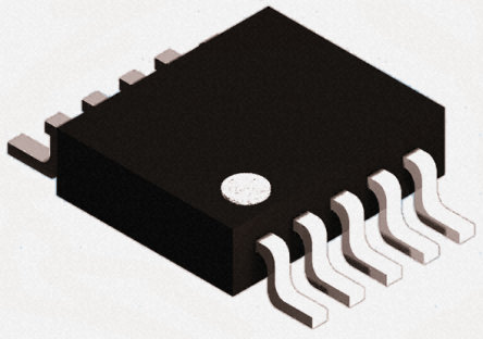
The AD5313R, a member of the _nano_DAC® family, is a low power, dual, 10-bit buffered voltage output digital-to-analog converter DAC. The device includes a 2.5 V, 2 ppm/°C internal reference enabled by default and a gain select pin giving a full-scale output of 2.5 V gain = 1 or 5 V gain = 2. The AD5313R operates from a single 2.7 V to 5.5 V supply, is guaranteed monotonic by design, and exhibits less than 0.1% FSR gain error and 1.5 mV offset error performance. The device is available in a 3 mm × 3 mm LFCSP package and a TSSOP package.
The AD5313R also incorporates a power-on reset circuit and a RSTSEL pin that ensures that the DAC outputs power up to zero scale or midscale and remain there until a valid write occurs. The part contains a per channel power-down feature that reduces the current consumption of the device to 4 μA at 3 V while in power-down mode.
The AD5313R employs a versatile serial peripheral interface SPI that operates at clock rates up to 50 MHz, and the device contains a VLOGIC pin that is intended for 1.8 V/3 V/5 V logic.
**Product Highlights**
1. Precision DC Performance.
Total unadjusted error: ±0.1% of FSR maximum
Offset error: ±1.5 mV maximum
Gain error: ±0.1% of FSR maximum
2. Low Drift 2.5 V On-Chip Reference.
2 ppm/°C typical temperature coefficient
5 ppm/°C maximum temperature coefficient
3. Two Package Options.
3 mm × 3 mm, 16-lead LFCSP
16-lead TSSOP
****Applications****
- .
- Optical transceivers
- .
- Base station power amplifiers
- .
- Process control PLC I/O cards
- .
- Industrial automation
- .
- Data acquisition systems
### Features and Benefits
- .
- Low drift 2.5 V reference: 2 ppm/°C typical
- .
- Tiny package: 3 mm × 3 mm, 16-lead LFCSP
- .
- Total unadjusted error TUE: ±0.1% of FSR maximum
- .
- Offset error: ±1.5 mV maximum
- .
- Gain error: ±0.1% of FSR maximum
- .
- High drive capability: 20 mA, 0.5 V from supply rails
- .
- User selectable gain of 1 or 2 GAIN pin
- .
- Reset to zero scale or midscale RSTSEL pin
- .
- 1.8 V logic compatibility
- .
- 50 MHz SPI with readback or daisy chain
- .
- Low glitch: 0.5 nV-sec
- .
- Low power: 3.3 mW at 3 V
- .
- 2.7 V to 5.5 V power supply
- .
- −40°C to +105°C temperature range