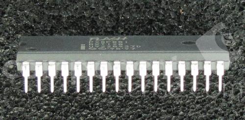
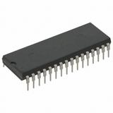
P28F001BX-B120
Flash Parallel 5V 1Mbit 128K x 8Bit 120ns 32Pin PDIP
’s 28F001BX-B and 28F001BX-T combine the cost-effectiveness of Intel standard flash memory with features that simplify write and allow block erase. These devices aid the system designer by combining the functions of several components into one, making boot block flash an innovative alternative to EPROM and EEPROM or battery-backed static RAM. Many new and existing designs can take advantage of the 28F001BX’s integration of blocked architecture, automated electrical reprogramming, and standard processor interface.
High-Integration Blocked Architecture
One 8 KB Boot Block w/Lock Out
Two 4 KB Parameter Blocks
One 112 KB Main Block
100,000 Erase/Program Cycles Per Block
Simplified Program and Erase
Automated Algorithms via On-Chip Write State Machine WSM
SRAM-Compatible Write Interface
Deep Power-Down Mode
0.05 mA ICC Typical
0.8 mA IPP Typical
12.0V g5% VPP
High-Performance Read
70/75 ns, 90 ns, 120 ns, 150 ns Maximum Access Time
5.0V g10% VCC
Hardware Data Protection Feature
Erase/Write Lockout during Power Transitions
Advanced Packaging, JEDEC Pinouts
32-Pin PDIP
32-Lead PLCC, TSOP
ETOXTM II Nonvolatile Flash Technology
EPROM-Compatible Process Base
High-Volume Manufacturing Experience
Extended Temperature Options