ADCLK954
两个可选的输入,12个LVPECL输出, SiGe半导体时钟扇出缓冲器 Two Selectable Inputs, 12 LVPECL Outputs, SiGe Clock Fanout Buffer
Product Details
The is an ultrafast clock fanout buffer fabricated on the Analog Devices, Inc., proprietary XFCB3 silicon germanium SiGe bipolar process. This device is designed for high speed applications requiring low jitter.
The device has two selectable differential inputs via the IN_SEL control pin. Both inputs are equipped with center tapped, differential, 100 Ω on-chip termination resistors. The inputs accept dc-coupled LVPECL, CML, 3.3 V CMOS single-ended, and ac-coupled 1.8 V CMOS, LVDS, and LVPECL inputs. A VREFx pin is available for biasing ac-coupled inputs.
The ADCLK954 features 12 full-swing emitter coupled logic ECL output drivers. For LVPECL positive ECL operation, bias Vcc to the positive supply and VEE to ground. For ECL operation, bias VCC to ground and VEE to the negative supply.
The output stages are designed to directly drive 800 mV each side into 50 Ω terminated to VCC − 2 V for a total differential output swing of 1.6 V.
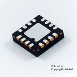
The ADCLK954 is available in a 40-lead LFCSP and specified for operation over the standard industrial temperature range of −40°C to +85°C.
**Applications**
* Low jitter clock distribution
* Clock and data signal restoration
* Level translation
* Wireless communications
* Wired communications
* Medical and industrial imaging
* ATE and high performance instrumentation
### Features and Benefits
- .
- 2 selectable differential inputs
- .
- 4.8 GHz operating frequency
- .
- 75 fs rms broadband random jitter
- .
- On-chip input terminations
- .
- 3.3 V power supply