USRP B210之FPAG分析6:确定硬件没有实际连接的端口
时间:2023-06-05 21:37:00
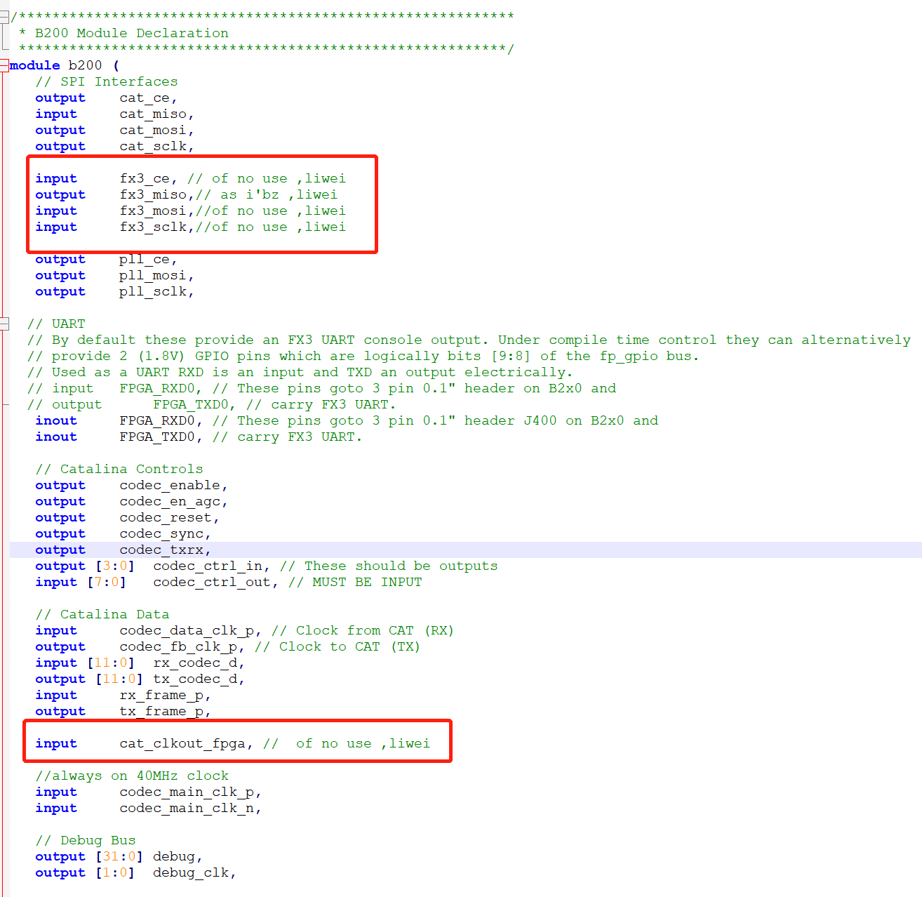
TOP层外接到FPGA有几个引脚不需要。首先,再次列出接口代码。
/*********************************************************** * B200 Module Declaration **********************************************************/ module b200 ( // SPI Interfaces output cat_ce, input cat_miso, output cat_mosi, output cat_sclk, input fx3_ce, output fx3_miso, input fx3_mosi, input fx3_sclk, output pll_ce, output pll_mosi, output pll_sclk, // UART // By default these provide an FX3 UART console output. Under compile time control they can alternatively // provide 2 (1.8V) GPIO pins which are logically bits [9:8] of the fp_gpio bus. // Used as a UART RXD is an input and TXD an output electrically. // input FPGA_RXD0, // These pins goto 3 pin 0.1" header on B2x0 and // output FPGA_TXD0, // carry FX3 UART. inout FPGA_RXD0, // These pins goto 3 pin 0.1" header J400 on B2x0 and inout FPGA_TXD0, // carry FX3 UART. // Catalina Controls output codec_enable, output codec_en_agc, output codec_reset, output codec_sync, output codec_txrx, output [3:0] codec_ctrl_in, // These should be outputs input [7:0] codec_ctrl_out, // MUST BE INPUT // Catalina Data input codec_data_clk_p, // Clock from CAT (RX) output codec_fb_clk_p, // Clock to CAT (TX) input [11:0] rx_codec_d, output [11:0] tx_codec_d, input rx_frame_p, output tx_frame_p, input cat_clkout_fpga, //always on 40MHz clock input codec_main_clk_p, input codec_main_clk_n, // Debug Bus output [31:0] debug, output [1:0] debug_clk, // GPIF, FX3 Slave FIFO output IFCLK, // pclk input FX3_EXTINT, output GPIF_CTL0, // n_slcs output GPIF_CTL1, // n_slwr output GPIF_CTL2, // n_sloe output GPIF_CTL3, // n_slrd output GPIF_CTL7, // n_pktend input GPIF_CTL4, // slfifo_flags[0] input GPIF_CTL5, // slfifo_flags[1] input GPIF_CTL6, // Serial settings bus from FX3. SDA input GPIF_CTL8, // Serial settings bus from FX3. SCL output GPIF_CTL11, // slfifo_addr[1] output GPIF_CTL12, // slfifo_addr[0] inout [31:0] GPIF_D, input GPIF_CTL9, // global_reset // GPS input gps_lock, output gps_rxd, input gps_txd, // FPGA has pullup for unpopulated GPS input gps_txd_nmea, // FPGA has pullup for unpopulated GPS // LEDS output LED_RX1, output LED_RX2, output LED_TXRX1_RX, output LED_TXRX1_TX, output LED_TXRX2_RX, output LED_TXRX2_TX, // GPIO Header J504 - 10 pin 0.1" 3.3V. // Only present on Rev6 and later boards...these pins unused on Rev5 and earlier. // NOTE: These pins are allocated from complimentry pairs and could potentially be used // as differential style I/O. `ifdef TARGET_B210 inout [7:0] fp_gpio, `endif // Misc Hardware Control output ref_sel, input pll_lock, input FPGA_CFG_CS, // Driven by FX3 gpio. input AUX_PWR_ON, // Driven by FX3 gpio. // PPS input PPS_IN_EXT, input PPS_IN_INT, // RF Hardware Control output SFDX1_RX, output SFDX1_TX, output SFDX2_RX, output SFDX2_TX, output SRX1_RX, output SRX1_TX, output SRX2_RX, output SRX2_TX, output tx_bandsel_a, output tx_bandsel_b, output tx_enable1, output tx_enable2, output rx_bandsel_a, output rx_bandsel_b, output rx_bandsel_c ); 以下截图列出不实际没有链接的接口信号:
一旦建成迷人的建筑,就要拆除凌乱的钢手脚。在标记了这些代码后,我们对整体结构更加清晰。这些引脚应该保留,否则FPGA默认输出可能会影响,FX3芯片。当然,自己画板的时候可以做可选的0欧电阻。实际生产后不焊接。


