DS90C365AMT
TEXAS INSTRUMENTS DS90C365AMT 总线, CAN, 收发器, 3 V, 3.6 V, TSSOP
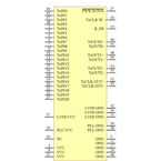
The is a Transmitter converts 21-bits of LVCMOS/LVTTL data into four LVDS low voltage differential signalling data streams. A phase-locked transmit clock is transmitted in parallel with the data streams over the fourth LVDS link. Every cycle of the transmit clock 21-bits RGB of input data are sampled and transmitted. At a transmit clock frequency of 87.5MHz, 21-bits of RGB data and 3-bits of LCD timing and control data FPLINE, FPFRAME, DRDY are transmitted at a rate of 612.5Mbps per LVDS data channel. Using a 87.5MHz clock, the data throughput is 229.687Mbps. This transmitter can be programmed for Rising edge strobe or falling edge strobe through a dedicated pin. A Rising edge or Falling edge strobe transmitter will interoperate with a Falling edge strobe FPDLink Receiver without any translation logic. This chipset is an ideal means to solve EMI and cable size problems associated with wide, high-speed TTL interfaces with added spread spectrum clocking support.
- .
- Pin-to-Pin-compatible to DS90C363, DS90C363A and DS90C365
- .
- No special start-up sequence required between clock/data and /PD pins
- .
- Supports spread spectrum clocking up to 100kHz frequency modulation
- .
- Narrow bus reduces cable size
- .
- Up to 1.785Gbps throughput
- .
- Up to 223.125Mbps bandwidth
- .
- 345mV Typical Swing LVDS devices for low EMI
- .
- PLL requires no external components
- .
- Compliant to A/EIA-644 LVDS standard
Device has limited built-in ESD protection. The leads should be shorted together or the device placed in conductive foam during storage or handling to prevent electrostatic damage to the MOS gates.