DS90C383BMT/NOPB
TEXAS INSTRUMENTS DS90C383BMT/NOPB 驱动器, LVDS, 发送器, 60 mA, -10 °C, 70 °C, 3 V
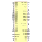
The is a programmable LVDS Transmitter converts 28 bits of CMOS/TTL data into four LVDS low voltage differential signalling data streams. A phase-locked transmit clock is transmitted in parallel with the data streams over a fifth LVDS link. Every cycle of the transmit clock 28 bits of input data are sampled and transmitted. At a transmit clock frequency of 65MHz, 24 bits of RGB data and 3 bits of LCD timing and control data FPLINE, FPFRAME, DRDY are transmitted at a rate of 455Mbps per LVDS data channel. Using a 65MHz clock, the data throughput is 227Mbps. The DS90C383B transmitter can be programmed for rising edge strobe or falling edge strobe through a dedicated pin. A rising edge or falling edge strobe transmitter will interoperate with a falling edge strobe receiver DS90CF386 without any translation logic. This chipset is an ideal means to solve EMI and cable size problems associated with wide, high speed TTL interfaces.
- .
- No special start-up sequence required between clock/data and /PD pins
- .
- Input signal clock and data can be applied either before or after the device is powered
- .
- Support spread spectrum clocking up to 100kHz frequency modulation
- .
- Deviations of ±2.5% centre spread or -5% down spread
- .
- Best-in-class set and hold times on TxINPUTs
- .
- Tx power consumption of <130mW typical at 65MHz grayscale
- .
- 40% Less power dissipation than BiCMOS alternatives
- .
- Tx Power-down mode of <60µW typical
- .
- Supports VGA, SVGA, XGA and dual pixel SXGA
- .
- Narrow bus reduces cable size
- .
- PLL requires no external components
- .
- 18 to 68MHz Shift clock support
- .
- 345mV Typical Swing LVDS devices for low EMI
- .
- Green product and no Sb/Br