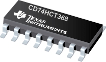
CD74HCT368
具有反向三态输出的高速 CMOS 逻辑六路缓冲器/线路驱动器
The HC367, HCT367, HC368, and silicon gate CMOS three-state buffers are general purpose high-speed non-inverting and inverting buffers. They have high drive current outputs which enable high speed operation even when driving large bus capacitances. These circuits possess the low power dissipation of CMOS circuitry, yet have speeds comparable to low power Schottky TTL circuits. Both circuits are capable of driving up to 15 low power Schottky inputs.
The HC367 and HCT367 are non-inverting buffers, whereas the HC368 and CD74HCT368 are inverting buffers. These devices have two output enables, one enable OE1 controls 4 gates and the other OE2 controls the remaining 2 gates.
The HCT367 and CD74HCT368 logic families are speed, function and pin compatible with the standard LS logic family.
- .
- Buffered Inputs
- .
- High Current Bus Driver Outputs
- .
- Two Independent Three-State Enable Controls
- .
- Typical Propagation Delay tPLH,tPHL = 8ns at VCC =5V, CL = 15pF, TA = 25°C
- .
- Fanout Over Temperature Range
- .
- Standard Outputs...10 LSTTL Loads
- .
- Bus Driver Outputs...15 LSTTL Loads
- .
- Wide Operating Temperature Range... 55°C to 125°C
- .
- Balanced Propagation Delay and Transition Times
- .
- Significant Power Reduction Compared to LSTTL Logic ICs
- .
- HC Types
- .
- 2V to 6V Operation
- .
- High Noise Immunity: NIL = 30%, NIH = 30% of VCC at VCC = 5V
- .
- HCT Types
- .
- 4.5V to 5.5V Operation
- .
- Direct LSTTL Input Logic Compatibility, VIL = 0.8V Max, VIH = 2V Min
- .
- CMOS Input Compatibility, I1 1µA at VOL, VOH
Data sheet acquired from Harris Semiconductor

