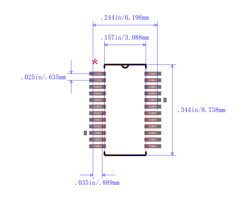
CDCFR83ADBQ
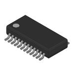
Direct Rambus™ 时钟发生器 24-SSOP -40 to 85
The Direct Rambus clock generator DRCG provides the necessary clock signals to support a Direct Rambus memory subsystem. It includes signals to synchronize the Direct Rambus channel clock to an external system or processor clock. It is designed to support Direct Rambus memory on a desktop, workstation, server, and mobile PC motherboards. DRCG also provides an off-the-shelf solution for a broad range of Direct Rambus memory applications.
The DRCG provides clock multiplication and phase alignment for a Direct Rambus memory subsystem to enable synchronous communication between the Rambus channel and ASIC clock domains. In a Direct Rambus memory subsystem, a system clock source provides the REFCLK and PCLK clock references to the DRCG and memory controller, respectively. The DRCG multiplies REFCLK and drives a high-speed BUSCLK to RDRAMs and the memory controller. Gear ratio logic in the memory controller divides the PCLK and BUSCLK frequencies by ratios M and N such that PCLKM = SYNCLKN, where SYNCLK = BUSCLK/4. The DRCG detects the phase difference between PCLKM and SYNCLKN and adjusts the phase of BUSCLK such that the skew between PCLKM and SYNCLKN is minimized. This allows data to be transferred across the SYNCLK/PCLK boundary without incurring additional latency.
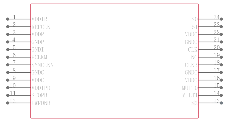
User control is provided by multiply and mode selection terminals. The multiply terminals provide selection of one of four clock frequency multiply ratios, generating BUSCLK frequencies ranging from 267 MHz to 533 MHz with clock references ranging from 33 MHz to 100 MHz. The mode select terminals can be used to select a bypass mode where the frequency multiplied reference clock is directly output to the Rambus channel for systems where synchronization between the Rambus clock and a system clock is not required. Test modes are provided to bypass the PLL and output REFCLK on the Rambus channel and to place the outputs in a high-impedance state for board testing.
The CDCFR83A has a fail-safe power up initialization state-machine which supports proper operation under all power up conditions.
The CDCFR83A is characterized for operation over free-air temperatures of 40°C to 85°C.