CDCVF2310MPWREP
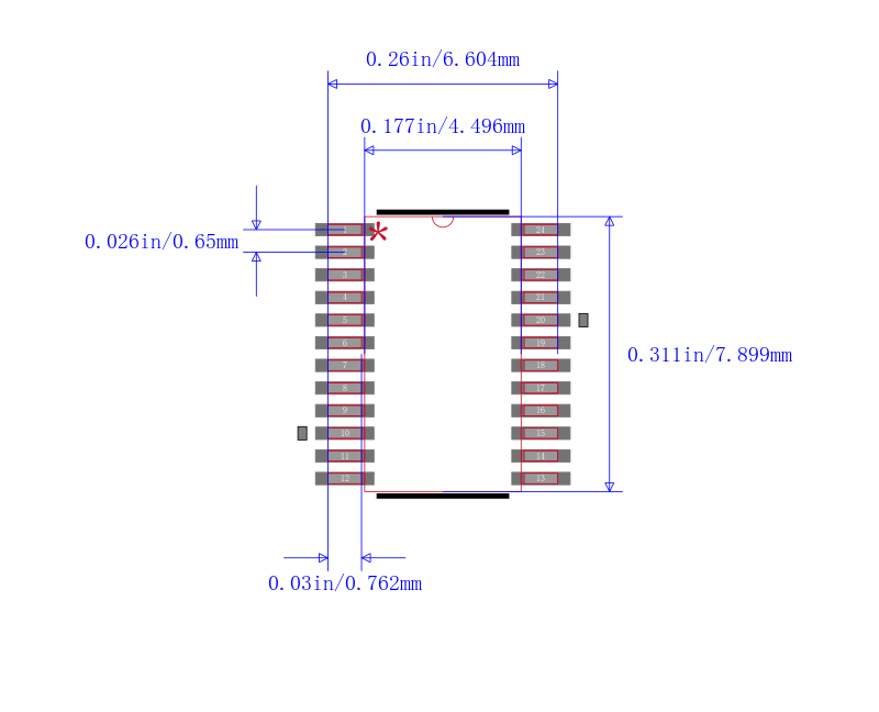
增强型产品 2.5V 至 3.3V 高性能时钟缓冲器 24-TSSOP -55 to 125
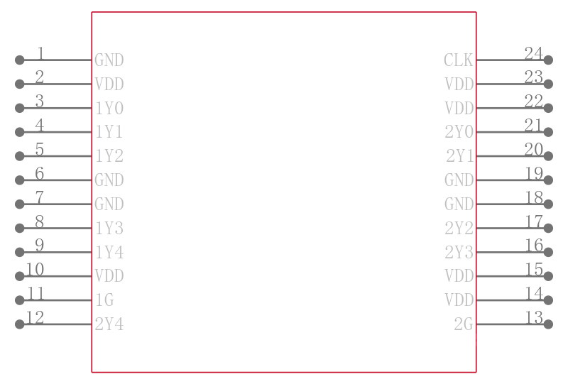
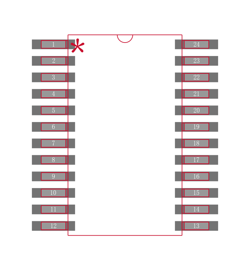
The CDCVF2310 is a high-performance, low-skew clock buffer that operates up to 200 MHz. Two banks of five outputs each provide low-skew copies of CLK. After power up, the default state of the outputs is low regardless of the state of the control pins. For normal operation, the outputs of bank 1Y[0:4] or 2Y[0:4] can be placed in a low state when the control pins 1G or 2G, respectively are held low and a negative clock edge is detected on the CLK input. The outputs of bank 1Y[0:4] or 2Y[0:4] can be switched into the buffer mode when the control pins 1G and 2G are held high and a negative clock edge is detected on the CLK input. The device operates in a 2.5-V and 3.3-V environment. The built-in output enable glitch suppression ensures a synchronized output enable sequence to distribute full period clock signals.
The CDCVF2310 is characterized for operation from 55°C to 125°C.