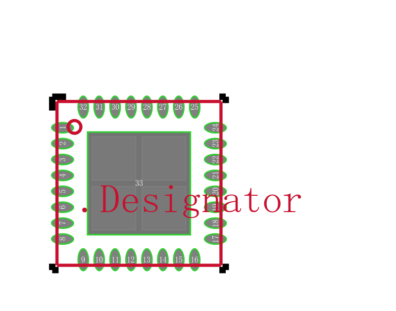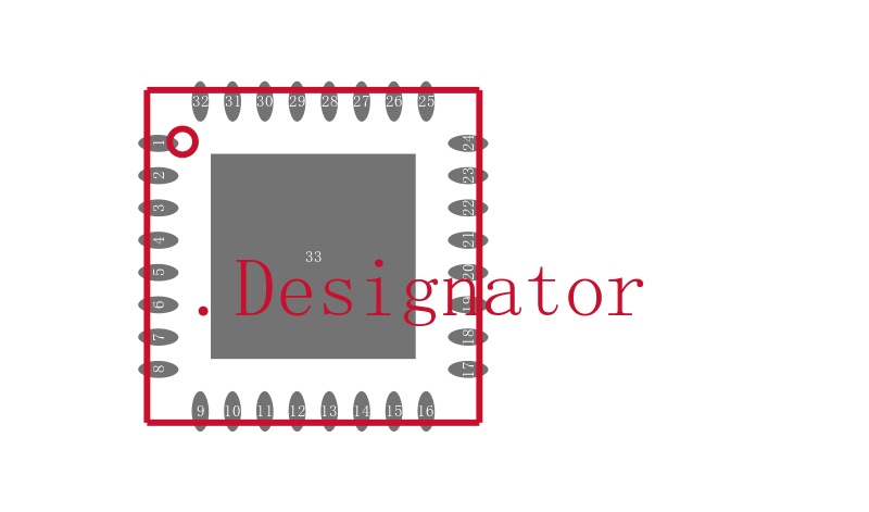
CDCLVC1310RHBR
TI(德州仪器)
主动器件
十大输出低抖动低功耗时钟缓冲器 Ten-Output Low-Jitter Low-Power Clock Buffer
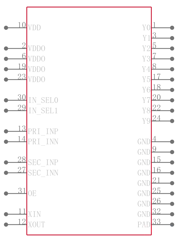
The is a highly versatile clock Fan-out Buffer can distribute to ten low-jitter LVCMOS clock outputs from one of three inputs, whose primary and secondary inputs can feature differential or single-ended signals and crystal input. Such a buffer is good for use in a variety of mobile and wired infrastructure applications. When the input is an illegal level, the output is at a defined state. Pin programming easily configures the CDCLVC1310. The overall additive jitter performance is 25fsRMS typical.
- .
- High-performance crystal buffer with ultra-low noise
- .
- Device inputs consist of primary, secondary, and crystal inputs and manually selectable
- .
- Differential and single-ended input frequencies supported are up to 200MHz
- .
- Synchronous and glitch-free output enable is available
- .
- 10 Single-ended LVCMOS outputs
- .
- LVCMOS Outputs Operate up to 200MHz
- .
- 30ps Typical output skew
- .
- Green product and no Sb/Br