CD4051BQPWRQ1
CMOS ALALOG多路复用器/多路解复用器采用逻辑电平转换 CMOS ALALOG MULTIPLEXERS/DEMULTIPLEXERS WITH LOGIC-LEVEL CONVERSION
The CD4051B, CD4052B, and CD4053B analog multiplexers are digitally-controlled analog switches that have low ON impedance and very low OFF leakage current. Control of analog signals up to 20 VP-P can be achieved by digital signal amplitudes of 4.5 V to 20 V If VDD \\- VSS = 3 V, a VDD \\- VEE of up to 13 V can be controlled; for VDD \\- VEE level differences above 13 V, a VDD \\- VSS of at least 4.5 V is required. For example, if VDD = 4.5 V, VSS = 0 V, and VEE = 13.5 V, analog signals from 13.5 V to 4.5 V can be controlled by digital inputs of 0 V to 5 V. These multiplexer circuits dissipate extremely low quiescent power over the full VDD \\- VSS and VDD \\- VEE supply-voltage ranges, independent of the logic state of the control signals. When a logic high H is present at the inhibit INH input, all channels are off.
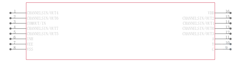
The CD4051B is a single eight-channel multiplexer that has three binary control inputs A, B, and C and an inhibit input. The three binary signals select one of eight channels to be turned on and connect one of the eight inputs to the output.
The CD4052B is a differential four-channel multiplexer that has two binary control inputs A and B and an inhibit input. The two binary input signals select one of four pairs of channels to be turned on and connect the analog inputs to the outputs.
The CD4053B is a triple two-channel multiplexer with three separate digital control inputs A, B, and C and an inhibit input. Each control input selects one of a pair of channels, which are connected in a single-pole, double-throw configuration.
When these devices are used as demultiplexers, the CHANNEL IN/OUT terminals are the outputs, and the common COM OUT/IN terminals are the inputs.