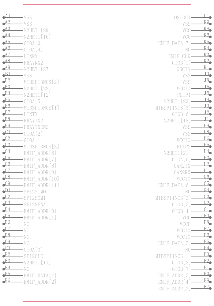
TMS5703137CGWTQEP
ARM微控制器 - MCU 16/32-Bit RISC Flash MCU
The TMS570LS3137-EP device is a high-performance microcontroller family for safety systems. The safety architecture includes the following:
The TMS570LS3137-EP device integrates the ARM Cortex-R4F Floating-Point CPU which offers an efficient 1.66 DMIPS/MHz, and has configurations which can run up to 180 MHz, providing up to 298 DMIPS. The device supports the word-invariant big-endian [BE32] format.
The TMS570LS3137-EP device has 3MB of integrated flash and 256KB of data RAM with single-bit error correction and double-bit error detection. The flash memory on this device is a nonvolatile, electrically erasable and programmable memory implemented with a 64-bit-wide data bus interface. The flash operates on a 3.3-V supply input same level as I/O supply for all read, program and erase operations. When in pipeline mode, the flash operates with a system clock frequency of up to 180 MHz. The SRAM supports single-cycle read and write accesses in byte, halfword, word and double-word modes.
The TMS570LS3137-EP device features peripherals for real-time control-based applications, including two Next Generation High-End Timer N2HET timing coprocessors and two 12-bit analog-to-digital converters ADCs supporting up to 24 inputs.
The N2HET is an advanced intelligent timer that provides sophisticated timing functions for real-time applications. The timer is software-controlled, using a reduced instruction set, with a specialized timer micromachine and an attached I/O port. The N2HET can be used for pulse-width-modulated outputs, capture or compare inputs, or GPIO. The N2HET is especially well suited for applications requiring multiple sensor information and drive actuators with complex and accurate time pulses. A High-End Timer Transfer Unit HTU can perform DMA-type transactions to transfer N2HET data to or from main memory. A Memory Protection Unit MPU is built into the HTU.
The device has two 12-bit-resolution MibADCs with 24 channels and 64 words of parity-protected buffer RAM each. The MibADC channels can be converted individually or can be grouped by software for sequential conversion sequences. Sixteen channels are shared between the two MibADCs. There are three separate groupings. Each sequence can be converted once when triggered or configured for continuous conversion mode.
The device has multiple communication interfaces: three MibSPIs, , one LIN, one SCI, three DCANs, one I2C. The SPIs provide a convenient method of serial high-speed communication between similar shift-register type devices. The LIN supports the Local Interconnect standard 2.0 and can be used as a UART in full-duplex mode using the standard Non-Return-to-Zero NRZ format.
The DCAN supports the CAN 2.0 A and B protocol standard and uses a serial, multimaster communication protocol that efficiently supports distributed real-time control with robust communication rates of up to 1 Mbps. The DCAN is ideal for systems operating in noisy and harsh environments for example, automotive vehicle networking and industrial fieldbus that require reliable serial communication or multiplexed wiring.
The I2C module is a multimaster communication module providing an interface between the microcontroller and an I2C-compatible device via the I2C serial bus. The I2C supports speeds of 100 and 400 Kbps.
The frequency-modulated phase-locked loop FMPLL clock module is used to multiply the external frequency reference to a higher frequency for internal use. There are two FMPLL modules on this device. These modules, when enabled, provide two of the seven possible clock source inputs to the global clock module GCM. The GCM manages the mapping between the available clock sources and the device clock domains.
The device also has an external clock prescaler ECP module that when enabled, outputs a continuous external clock on the ECLK pin/ball. The ECLK frequency is a user-programmable ratio of the peripheral interface clock VCLK frequency. This low-frequency output can be monitored externally as an indicator of the device operating frequency.
The DMA controller has 16 channels, 32 control packets and parity protection on its memory. An MPU is built into the DMA to limit the DMA to prescribed areas of memory and to protect the rest of the memory system from any malfunction of the DMA.
The Error Signaling Module ESM monitors all device errors and determines whether an interrupt is generated or the external ERROR pin is toggled when a fault is detected. The ERROR pin can be monitored externally as an indicator of a fault condition in the microcontroller.
The External Memory Interface EMIF provides off-chip expansion capability with the ability to interface to synchronous DRAM SDRAM devices, asynchronous memories, peripherals or FPGA devices.
Several interfaces are implemented to enhance the debugging capabilities of application code. In addition to the built in ARM Cortex-R4F CoreSight debug features an External Trace Macrocell ETM provides instruction and data trace of program execution. For instrumentation purposes, a RAM Trace Port RTP module is implemented to support high-speed tracing of RAM and peripheral accesses by the CPU or any other master. A Data Modification Module DMM gives the ability to write external data into the device memory. Both the RTP and DMM have no or only minimum impact on the program execution time of the application code. A Parameter Overlay Module POM can reroute flash accesses to internal memory or to the EMIF. This rerouting allows parameters and tables to be dynamically calibrated against production code without rebuilding the code to explicitly access RAM or halting the processor to reprogram the data flash.
With integrated safety features and a wide choice of communication and control peripherals, the device is an ideal solution for high-performance real-time control applications with safety-critical requirements.