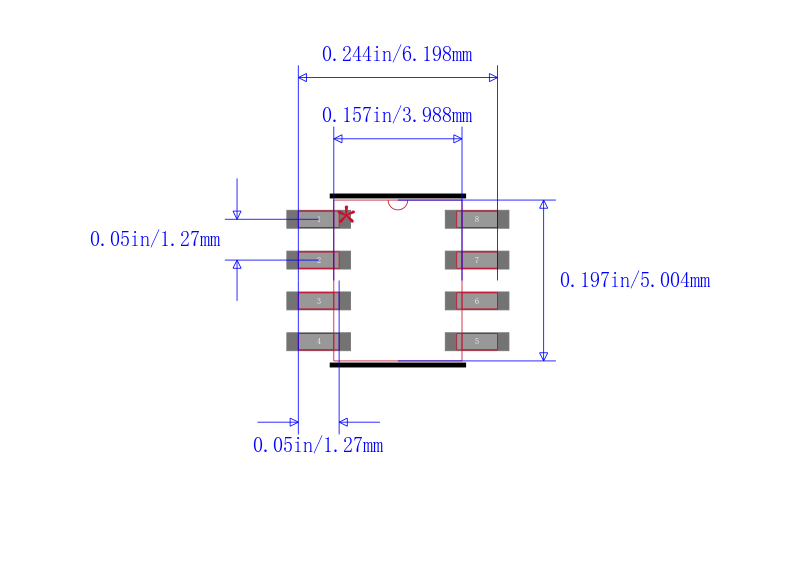
TLV5606CDR
2.7 V至WITH POWER DOWN 5.5 V低功耗10位数字 - 模拟转换器 2.7 V TO 5.5 V LOW POWER 10-BIT DIGITAL-TO-ANALOG CONVERTERS WITH POWER DOWN
description
The TLV5606 is a 10-bit voltage output digital-to-analog converter DAC with a flexible 4-wire serial interface. The 4-wire serial interface allows glueless interface to TMS320, SPI, QSPI, and Microwire serial ports. The TLV5606 is programmed with a 16-bit serial string containing 4 control and 10 data bits. Developed for a wide range of supply voltages, the TLV5606 can operate from 2.7 V to 5.5 V.
The resistor string output voltage is buffered by a x2 gain rail-to-rail output buffer. The buffer features a Class AB output stage to improve stability and reduce settling time. The settling time of the DAC is programmable to allow the designer to optimize speed versus power dissipation. The settling time is chosen by the control bits within the 16-bit serial input string. A high-impedance buffer is integrated on the REFIN terminal to reduce the need for a low source impedance drive to the terminal.
Implemented with a CMOS process, the TLV5606 is designed for single supply operation from 2.7 V to 5.5 V. The device is available in an 8-terminal SOIC package. The TLV5606C is characterized for operation from 0°C to 70°C. The TLV5606I is characterized for operation from −40°C to 85°C.
features
• 10-Bit Voltage Output DAC
• Programmable Settling Time vs Power Consumption
3 µs in Fast Mode
9 µs in Slow Mode
• Ultra Low Power Consumption:
900 µW Typ in Slow Mode at 3 V
2.1 mW Typ in Fast Mode at 3 V
• Differential Nonlinearity . . . <0.2 LSB Typ
• Compatible With TMS320 and SPI Serial Ports
• Power-Down Mode 10 nA
• Buffered High-Impedance Reference Input
• Voltage Output Range . . . 2 Times the Reference Input Voltage
• Monotonic Over Temperature
• Available in MSOP Package
applications
• Digital Servo Control Loops
• Digital Offset and Gain Adjustment
• Industrial Process Control
• Machine and Motion Control Devices
• Mass Storage Devices


