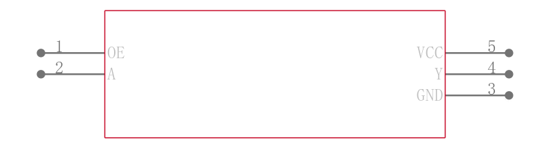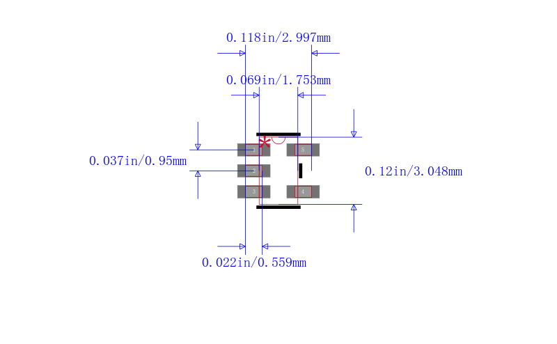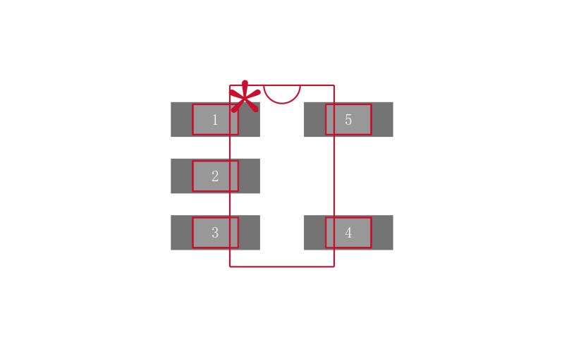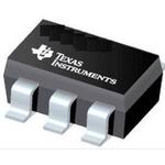
SN74AHCT1G126DBVR
TI(德州仪器)
电子元器件分类
单总线缓冲,三态输出
The is a single Bus Buffer Gate/Line Driver with 3-state output. The output is disabled when the output-enable OE input is low. When OE is high, true data is passed from the A input to the Y output. To ensure the high-impedance state during power up or power down, OE should be tied to GND through a pull-down resistor and the minimum value of the resistor is determined by the current-sourcing capability of the driver.
- .
- Inputs are TTL-voltage compatible
- .
- Slow edges reduce output ringing
- .
- TTL inputs - Lowered switching threshold allows up translation 3.3 to 5V
- .
- 10µA maximum ICC low power consumption
- .
- 6ns at 5V Propagation delay tpd
- .
- ±8mA Output drive at 5V
- .
- Latch-up performance exceeds 250mA per JESD 17
- .
- Green product and no Sb/Br