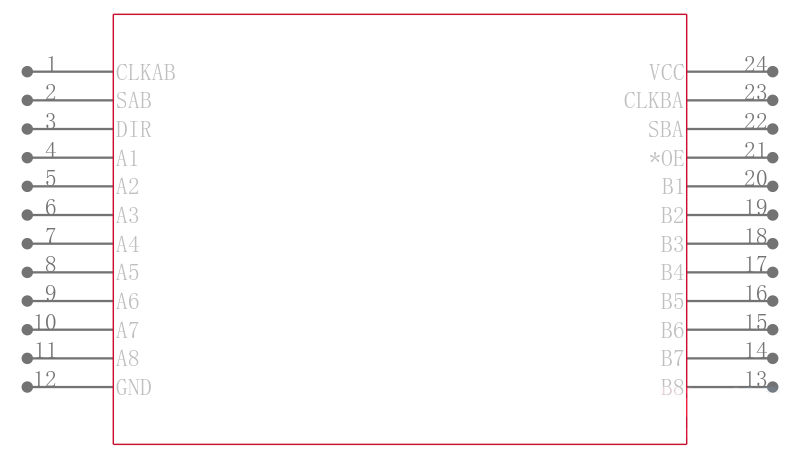
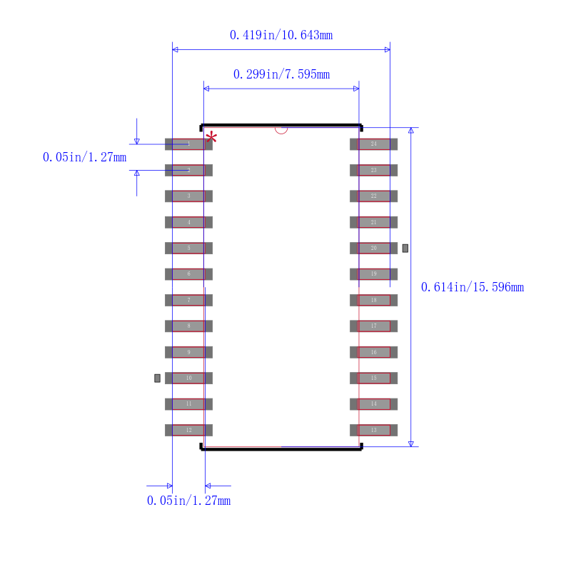
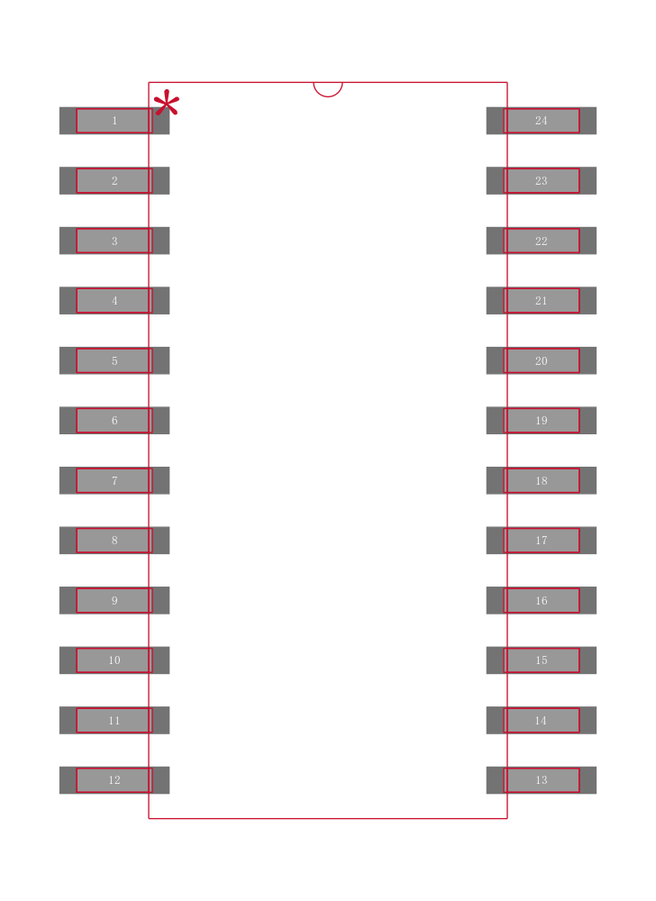
SN74LVTH646DWR
IC BUS TRANSCEIVER 8Bit 24SOIC
description/ordering information
These bus transceivers and registers are designed specifically for low-voltage 3.3-V VCC operation, but with the capability to provide a TTL interface to a 5-V system environment.
The ’LVTH646 devices consist of bus transceiver circuits, D-type flip-flops, and control circuitry arranged for multiplexed transmission of data directly from the input bus or from the internal registers. Data on the A or B bus is clocked into the registers on the low-to-high transition of the appropriate clock CLKAB or CLKBA input. Figure 1 illustrates the four fundamental bus-management functions that can be performed with the ’LVTH646.
• Support Mixed-Mode Signal Operation
5-V Input and Output Voltages With 3.3-V VCC
• Support Unregulated Battery Operation Down to 2.7 V
• Typical VOLP Output Ground Bounce
<0.8 V at VCC = 3.3 V, TA = 25°C
• Ioff and Power-Up 3-State Support Hot Insertion
• Bus Hold on Data Inputs Eliminates the Need for External Pullup/Pulldown Resistors
• Latch-Up Performance Exceeds 500 mA Per JESD 17
• ESD Protection Exceeds JESD 22
− 2000-V Human-Body Model A114-A
− 200-V Machine Model A115-A


