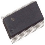
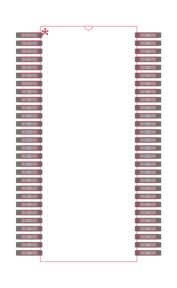
SN74ALVCH16823DLR
具有三态输出的 18 位总线接口触发器 56-SSOP -40 to 85
This 18-bit bus-interface flip-flop is designed for 1.65-V to 3.6-V VCC operation.
The SN74ALVCH16823 features 3-state outputs designed specifically for driving highly capacitive or relatively low-impedance loads. This device is particularly suitable for implementing wider buffer registers, I/O ports, bidirectional bus drivers with parity, and working registers.
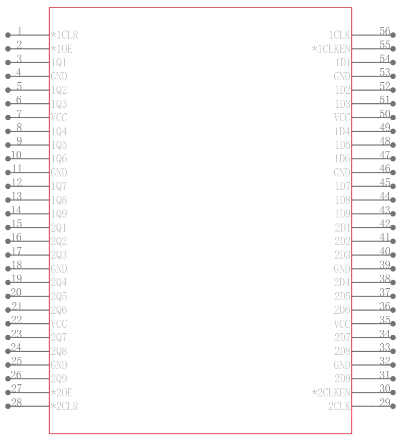
The SN74ALVCH16823 can be used as two 9-bit flip-flops or one 18-bit flip-flop. With the clock-enable CLKEN input low, the D-type flip-flops enter data on the low-to-high transitions of the clock. Taking CLKEN high disables the clock buffer, thus latching the outputs. Taking the clear CLR input low causes the Q outputs to go low independently of the clock.
A buffered output-enable OE input can be used to place the nine outputs in either a normal logic state high or low logic levels or the high-impedance state. In the high-impedance state, the outputs neither load nor drive the bus lines significantly. The high-impedance state and increased drive provide the capability to drive bus lines without need for interface or pullup components.
The output-enable OE input does not affect the internal operation of the flip-flops. Old data can be retained or new data can be entered while the outputs are in the high-impedance state.
To ensure the high-impedance state during power up or power down, OE should be tied to VCC through a pullup resistor; the minimum value of the resistor is determined by the current-sinking capability of the driver.
Active bus-hold circuitry is provided to hold unused or floating data inputs at a valid logic level.
The SN74ALVCH16823 is characterized for operation from -40°C to 85°C.


