SN74LVTH574IPWREP
具有三态输出的增强型产品 3.3V Abt 八路边沿触发式 D 型触发器 20-TSSOP -40 to 85
This octal flip-flop is designed specifically for low-voltage 3.3-V VCC operation, but with the capability to provide a TTL interface to a 5-V system environment.
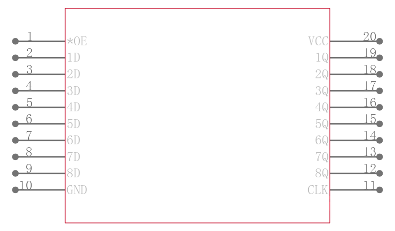
The eight flip-flops of the SN74LVTH574 are edge-triggered D-type flip-flops. On the positive transition of the clock CLK input, the Q outputs are set to the logic levels set up at the data D inputs.
A buffered output-enable OE\ input can be used to place the eight outputs in either a normal logic state high or low logic levels or a high-impedance state. In the high-impedance state, the outputs neither load nor drive the bus lines significantly. The high-impedance state and increased drive provide the capability to drive bus lines without need for interface or pullup components.
OE\ does not affect the internal operations of the flip-flops. Old data can be retained or new data can be entered while the outputs are in the high-impedance state.
To ensure the high-impedance state during power up or power down, OE\ should be tied to VCC through a pullup resistor; the minimum value of the resistor is determined by the current-sinking capability of the driver.
Active bus-hold circuitry is provided to hold unused or floating data inputs at a valid logic level. Use of pullup or pulldown resistors with the bus-hold circuitry is not recommended.
This device is fully specified for hot-insertion applications using Ioff and power-up 3-state. The Ioff circuitry disables the outputs, preventing damaging current backflow through the devices when they are powered down. The power-up 3-state circuitry places the outputs in the high-impedance state during power up and power down, which prevents driver conflict.


