锐单电子商城 , 一站式电子元器件采购平台!
  • 电话:400-990-0325

SN74LV574ADGVR

SN74LV574ADGVR

TI(德州仪器) 主动器件

八路边沿触发D型触发器具有​​三态输出 OCTAL EDGE-TRIGGERED D-TYPE FLIP-FLOPS WITH 3-STATE OUTPUTS

description/ordering information

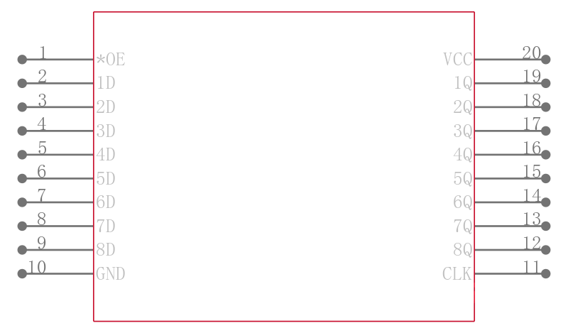
The ’LV574A devices are octal edge-triggered D-type flip-flops designed for 2-V to 5.5-V VCC operation.

These devices feature 3-state outputs designed specifically for driving highly capacitive or relatively low-impedance loads. The devices are particularly suitable for implementing buffer registers, I/O ports, bidirectional bus drivers, and working registers.

On the positive transition of the clock CLK input, the Q outputs are set to the logic levels set up at the data D inputs.

A buffered output-enable OE input can be used to place the eight outputs in either a normal logic state high or low logic levels or high-impedance state. In the high-impedance state, the outputs neither load nor drive the bus lines significantly. The high-impedance state and increased drive provide the capability to drive bus lines without need for interface or pullup components.

2-V to 5.5-V VCCOperation

Max tpdof 10 ns at 5 V

Typical VOLPOutput Ground Bounce

  <0.8 V at VCC= 3.3 V, TA= 25°C

Typical VOHVOutput VOHUndershoot

  >2.3 V at VCC= 3.3 V, TA= 25°C

Support Mixed-Mode Voltage Operation on All Ports

Ioff Supports Partial-Power-Down Mode Operation

Latch-Up Performance Exceeds 250 mA Per JESD 17

ESD Protection Exceeds JESD 22

− 2000-V Human-Body Model A114-A

− 200-V Machine Model A115-A

− 1000-V Charged-Device Model C101

SN74LV574ADGVR中文资料参数规格
技术参数

频率 175 MHz

电源电压DC 5.00 V, 5.50 V max

输出电流 16.0 mA

电路数 8

通道数 8

时钟频率 175 MHz

位数 8

极性 Non-Inverting

电压波节 5.00 V, 3.30 V, 2.50 V

输入电容 1.8 pF

工作温度Max 85 ℃

工作温度Min -40 ℃

电源电压 2V ~ 5.5V

电源电压Max 5.5 V

电源电压Min 2 V

封装参数

安装方式 Surface Mount

引脚数 20

封装 TFSOP-20

外形尺寸

宽度 4.4 mm

封装 TFSOP-20

物理参数

工作温度 -40℃ ~ 85℃ TA

其他

产品生命周期 Active

包装方式 Tape & Reel TR

符合标准

RoHS标准 RoHS Compliant

含铅标准 Lead Free

海关信息

ECCN代码 EAR99

SN74LV574ADGVR引脚图与封装图
SN74LV574ADGVR引脚图

SN74LV574ADGVR引脚图

SN74LV574ADGVR封装图

SN74LV574ADGVR封装图

SN74LV574ADGVR封装焊盘图

SN74LV574ADGVR封装焊盘图

在线购买SN74LV574ADGVR
型号 制造商 描述 购买
SN74LV574ADGVR TI 德州仪器 八路边沿触发D型触发器具有​​三态输出 OCTAL EDGE-TRIGGERED D-TYPE FLIP-FLOPS WITH 3-STATE OUTPUTS 搜索库存
替代型号SN74LV574ADGVR
图片 型号/品牌/封装 代替类型 描述 替代型号对比

型号: SN74LV574ADGVR

品牌: TI 德州仪器

封装: TVSOP-20 8Bit 5V 20Pin

当前型号

八路边沿触发D型触发器具有​​三态输出 OCTAL EDGE-TRIGGERED D-TYPE FLIP-FLOPS WITH 3-STATE OUTPUTS

当前型号

型号: SN74LV574APWRG4

品牌: 德州仪器

封装: 20-TSSOP 8Bit 20Pin

完全替代

Flip Flop D-Type Bus Interface Pos-Edge 3-ST 1Element 20Pin TSSOP T/R

SN74LV574ADGVR和SN74LV574APWRG4的区别

型号: SN74LV574ADGVRE4

品牌: 德州仪器

封装: 20Pin

完全替代

八路边沿触发D型触发器具有​​三态输出 OCTAL EDGE-TRIGGERED D-TYPE FLIP-FLOPS WITH 3-STATE OUTPUTS

SN74LV574ADGVR和SN74LV574ADGVRE4的区别

型号: SN74LV574APWR

品牌: 德州仪器

封装: TSSOP-20 8Bit 5V 20Pin

类似代替

74LV 系列,Texas Instruments低电压 CMOS 逻辑 工作电压:2 - 5.5 兼容性:输入 LVTTL/TTL、输出 LVCMOS ### 74LV 系列

SN74LV574ADGVR和SN74LV574APWR的区别