SN74LVC3G17YZPR
TRIPLE施密特触发缓冲器 TRIPLE SCHMITT TRIGGER BUFFER
description/ordering information
This triple Schmitt-trigger buffer is designed for 1.65-V to 5.5-V VCCoperation.
The SN74LVC3G17 contains three buffers, and performs the Boolean function Y = A. The device functions as three independent buffers, but because of Schmitt action, it may have different input threshold levels for positive-going VT+ and negative-going VT− signals.
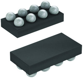
Available in the Texas Instruments NanoStar™ and NanoFreePackages
Supports 5-V VCCOperation
Inputs Accept Voltages to 5.5 V
Max tpdof 5.4 ns at 3.3 V
Low Power Consumption, 10-µA Max ICC
±24-mA Output Drive at 3.3 V
Typical VOLPOutput Ground Bounce <0.8 V at VCC= 3.3 V, TA= 25°C
Typical VOHVOutput VOHUndershoot >2 V at VCC= 3.3 V, TA= 25°C
Ioff Supports Partial-Power-Down Mode Operation
Latch-Up Performance Exceeds 100 mA Per JESD 78, Class II
ESD Protection Exceeds JESD 22
− 2000-V Human-Body Model A114-A
− 200-V Machine Model A115-A
− 1000-V Charged-Device Model C101


