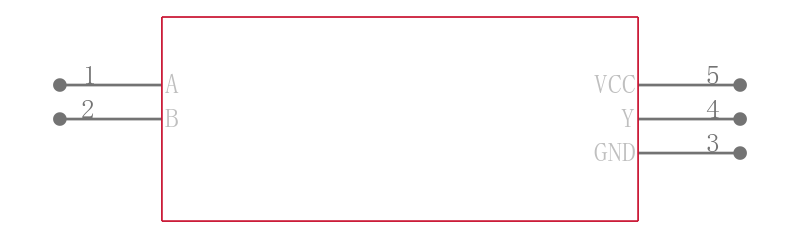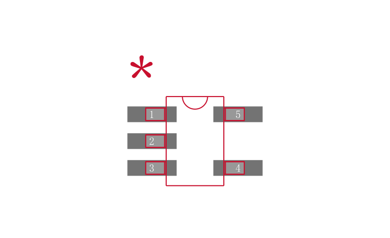
SN74AUP1T02DCKR
低功耗, 1.8 / 2.5 / 3.3 V输入, 3.3 V CMOS输出,单路2输入正或非门 LOW POWER, 1.8/2.5/3.3-V INPUT, 3.3-V CMOS OUTPUT,SINGLE 2-INPUT POSITIVE-NOR GATE
DESCRIPON/ORDERING INFORMATION
The SN74AUP1T02 performs the Boolean function Y = A + B or Y = A ● B with designation for logic-level translation applications with output referenced to supply VCC..
AUP technology is the industry"s lowest-power logic technology designed for use in extending battery-life in operating. All input levels that accept 1.8-V LVCMOS signals, while operating from either a single 3.3-V or 2.5-V VCC supply. This product also maintains excellent signal integrity see Figure 1 and Figure 2.
FEATURES
• Single-Supply Voltage Translator
• Output Level Up to Supply VCC CMOS Level
– 1.8 V to 3.3 V at VCC = 3.3 V
– 2.5 V to 3.3 V at VCC = 3.3 V
– 1.8 V to 2.5 V at VCC = 2.5 V
– 3.3 V to 2.5 V at VCC = 2.5 V
• Schmitt-Trigger Inputs Reject Input Noise and Provide Better Output Signal Integrity
• Ioff Supports Partial Power Down VCC = 0 V
• Very Low Static Power Consumption: 0.1 µA
• Very Low Dynamic Power Consumption: 0.9 µA
• Latch-Up Performance Exceeds 100 mA Per JESD 78, Class II
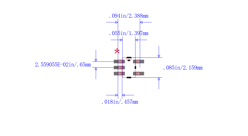
• Pb-Free Packages Available: SC-70 DCK 2 x 2.1 x 0.65 mm Height 1.1 mm
• More Gate Options Available at www.ti.com/littlelogic
• ESD Performance Tested Per JESD 22
– 2000-V Human-Body Model A114-B, Class II
– 1000-V Charged-Device Model C101