SN74CBT6800CDWR
具有 –2V 下冲保护的 5V、1:1 SPST、10 通道通用 FET 总线开关 24-SOIC -40 to 85
The SN74CBT6800C is a high-speed TTL-compatible FET bus switch with low ON-state resistance ron, allowing for minimal propagation delay. Active Undershoot-Protection Circuitry on the A and B ports of the SN74CBT6800C provides protection for undershoot up to 2 V by sensing an undershoot event and ensuring that the switch remains in the proper OFF state. The device also precharges the B port to a user-selectable bias voltage BIASV to minimize live-insertion noise.
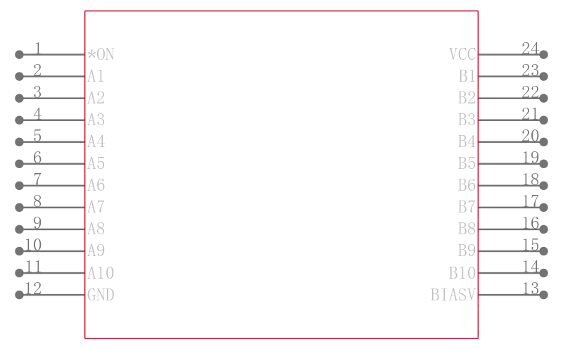
The SN74CBT6800C is a 10-bit bus switch with a single output-enable ON\\\\ input. When ON\ is low, the 10-bit bus switch is ON, and the A port is connected to the B port, allowing bidirectional data flow between ports. When ON\ is high, the 10-bit bus switch is OFF, and a high-impedance state exists between the A and B ports. The B port is precharged to BIASV through the equivalent of a 10-k resistor when ON\ is high, or if the device is powered down VCC = 0 V.
During insertion or removal of a card into or from an active bus, the cards output voltage may be close to GND. When the connector pins make contact, the cards parasitic capacitance tries to force the bus signal to GND, creating a possible glitch on the active bus. This glitching effect can be reduced by using a bus switch with precharged bias voltage BIASV of the bus switch equal to the input threshold voltage level of the receivers on the active bus. This method will ensure that any glitch produced by insertion or removal of the card will not cross the input threshold region of the receivers on the active bus, minimizing the effects of live-insertion noise.
This device is fully specified for partial-power-down applications using Ioff. The Ioff feature ensures that damaging current will not backflow through the device when it is powered down. The device has isolation during power off.
To ensure the high-impedance state during power up or power down, ON\ should be tied to VCC through a pullup resistor; the minimum value of the resistor is determined by the current-sinking capability of the driver.