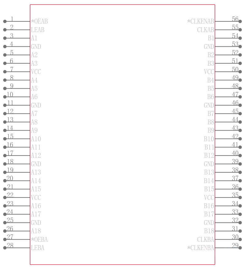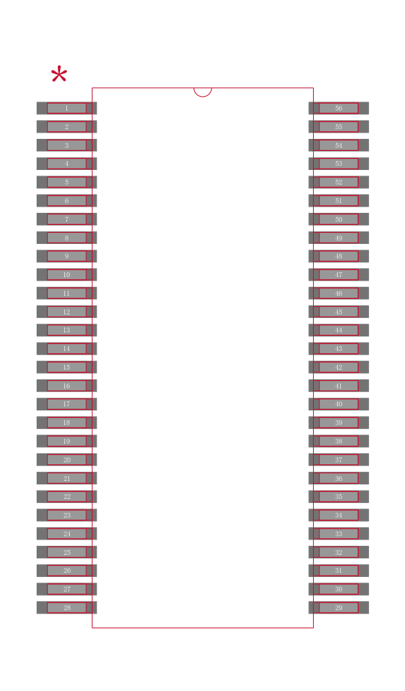
SN74ABT16601DL
18位通用总线收发器与3态输出 18-BIT UNIVERSAL BUS TRANSCEIVERS WITH 3-STATE OUTPUTS
These 18-bit universal bus transceivers combine D-type latches and D-type flip-flops to allow data flow in transparent, latched, clocked, and clock-enabled modes.
Data flow in each direction is controlled by output-enable and , latch-enable LEAB and LEBA, and clock CLKAB and CLKBA inputs. The clock can be controlled by the clock-enable and inputs. For A-to-B data flow, the device operates in the transparent mode when LEAB is high. When LEAB is low, the A data is latched if CLKAB is held at a high or low logic level. If LEAB is low, the A data is stored in the latch/flip-flop on the low-to-high transition of CLKAB. Output enable is active low. When is low, the outputs are active. When is high, the outputs are in the high-impedance state.
Data flow for B to A is similar to that of A to B, but uses , LEBA, CLKBA, and .
To ensure the high-impedance state during power up or power down, should be tied to VCC through a pullup resistor; the minimum value of the resistor is determined by the current-sinking capability of the driver.
The SN54ABT16601 is characterized for operation over the full military temperature range of -55°C to 125°C. The SN74ABT16601 is characterized for operation from -40°C to 85°C.