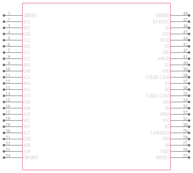
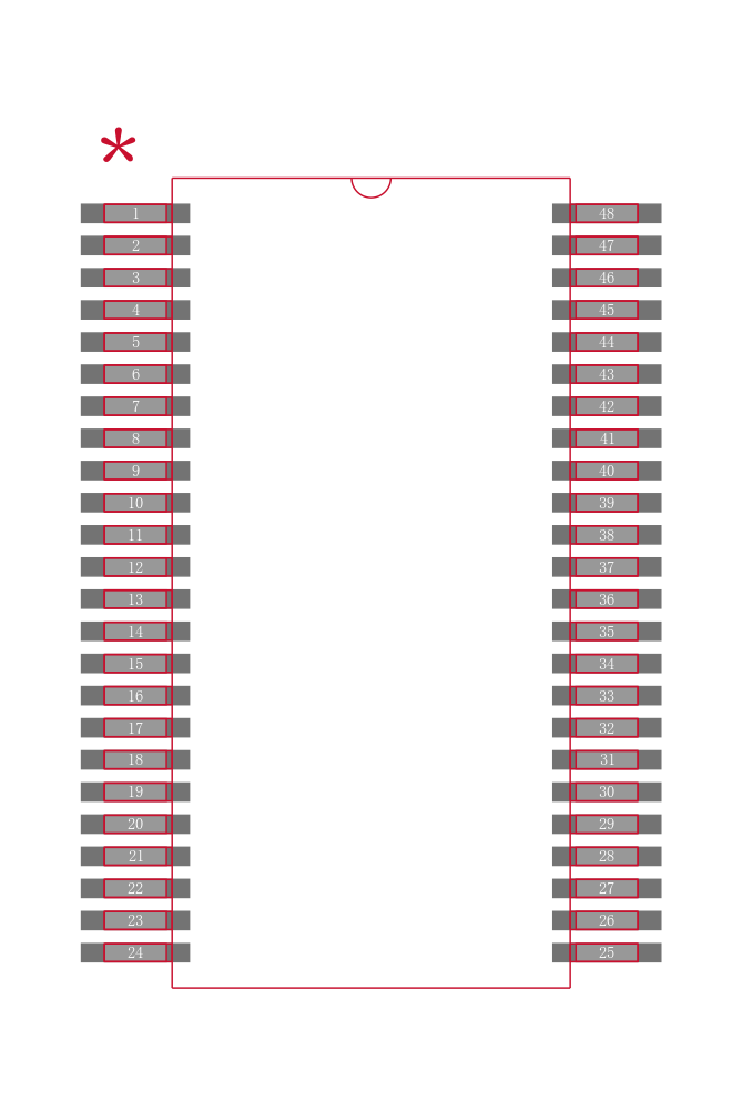
SN74GTLP2033DGGR
8位LVTTL至GTLP可调节边沿速率寄存收发器配劈开LVTTL端口和反馈路径 8-BIT LVTTL-TO-GTLP ADJUSTABLE-EDGE-RATE REGISTERED TRANSCEIVER WITH SPLIT LVTTL PORT AND FEEDBACK PATH
The SN74GTLP2033 is a high-drive, 8-bit, three-wire registered transceiver that provides inverted LVTTL-to-GTLP and GTLP-to-LVTTL signal-level translation. The device allows for transparent, latched, and flip-flop modes of data transfer with separate LVTTL input and LVTTL output pins, which provides a feedback path for control and diagnostics monitoring, the same functionality as the SN74FB2033. The device provides a high-speed interface between cards operating at LVTTL logic levels and a backplane operating at GTLP signal levels. High-speed about three times faster than standard LVTTL or TTL backplane operation is a direct result of GTLP"s reduced output swing <1 V, reduced input threshold levels, improved differential input, OEC circuitry, and -OPC circuitry. Improved GTLP OEC and TI-OPC circuits minimize bus-settling time and have been designed and tested using several backplane models. The high drive allows incident-wave switching in heavily loaded backplanes with equivalent load impedance down to 11 .
GTLP is the Texas Instruments derivative of the Gunning Transceiver Logic GTL JEDEC standard JESD 8-3. The ac specification of the SN74GTLP2033 is given only at the preferred higher noise-margin GTLP, but the user has the flexibility of using this device at either GTL VTT = 1.2 V and VREF = 0.8 V or GTLP VTT = 1.5 V and VREF = 1 V signal levels. For information on using GTLP devices in FB+/BTL applications, refer to TI application reports, _Texas Instruments GTLP Frequently Asked Questions_, literature number SCEA019, and _GTLP in BTL Applications_, literature number SCEA017.
Normally, the B port operates at GTLP signal levels. The A-port and control inputs operate at LVTTL logic levels, but are 5-V tolerant and can be directly driven by TTL or 5-V CMOS devices. VREF is the B-port differential input reference voltage.
This device is fully specified for live-insertion applications using Ioff, power-up 3-state, and BIAS VCC. The Ioff circuitry disables the outputs, preventing damaging current backflow through the device when it is powered down. The power-up 3-state circuitry places the outputs in the high-impedance state during power up and power down, which prevents driver conflict. The BIAS VCC circuitry precharges and preconditions the B-port input/output connections, preventing disturbance of active data on the backplane during card insertion or removal, and permits true live-insertion capability.
This GTLP device features TI-OPC circuitry, which actively limits overshoot caused by improperly terminated backplanes, unevenly distributed cards, or empty slots during low-to-high signal transitions. This improves signal integrity, which allows adequate noise margin to be maintained at higher frequencies.
High-drive GTLP backplane interface devices feature adjustable edge-rate control ERC. Changing the ERC input voltage between low and high adjusts the B-port output rise and fall times.This allows the designer to optimize system data-transfer rate and signal integrity to the backplane load.
When VCC is between 0 and 1.5 V, the device is in the high-impedance state during power up or power down. However, to ensure the high-impedance state above 1.5 V, OEAB\ should be tied to VCC through a pullup resistor and OEAB and OEBA should be tied to GND through a pulldown resistor; the minimum value of the resistor is determined by the current-sinking/current-sourcing capability of the driver. View datasheet View product folder


