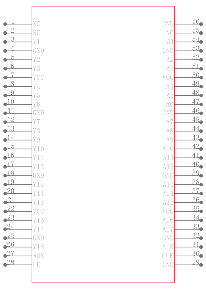
SN74LVTH16835DGGR
具有三态输出的 3.3V ABT 18 位通用总线驱动器 56-TSSOP -40 to 85
The "LVTH16835 devices are 18-bit universal bus drivers designed for low-voltage 3.3-V VCC operation, but with the capability to provide a TTL interface to a 5-V system environment.
Data flow from A to Y is controlled by the output-enable OE\\\\ input. These devices operate in the transparent mode when the latch-enable LE input is high. The A data is latched if the clock CLK input is held at a high or low logic level. If LE is low, the A data is stored in the latch/flip-flop on the low-to-high transition of the clock. When OE\ is high, the outputs are in the high-impedance state.
Active bus-hold circuitry is provided to hold unused or floating data inputs at a valid logic level.
When VCC is between 0 and 1.5 V, the devices are in the high-impedance state during power up or power down. However, to ensure the high-impedance state above 1.5 V, OE\ should be tied to VCC through a pullup resistor; the minimum value of the resistor is determined by the current-sinking capability of the driver.
These devices are fully specified for hot-insertion applications using Ioff and power-up 3-state. The Ioff circuitry disables the outputs, preventing damaging current backflow through the devices when they are powered down. The power-up 3-state circuitry places the outputs in the high-impedance state during power up and power down, which prevents driver conflict.
The SN54LVTH16835 is characterized for operation over the full military temperature range of -55°C to 125°C. The SN74LVTH16835 is characterized for operation from -40°C to 85°C.