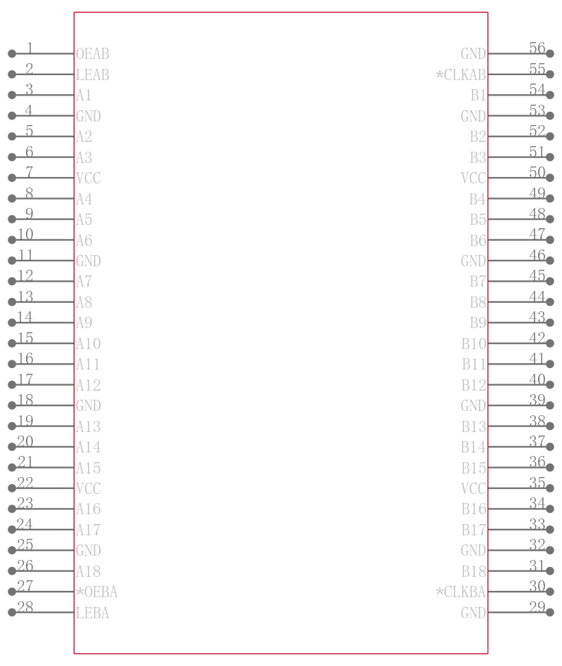
SN74LVTH16500DGGR
3.3 -V ABT 18位通用总线和三态输出收发器 3.3-V ABT 18-BIT UNIVERSAL BUS TRANSCEIVERS WITH 3-STATE OUTPUTS
The LVTH16500 devices are 18-bit universal bus transceivers designed for low-voltage 3.3-V VCC operation, but with the capability to provide a TTL interface to a 5-V system environment.
Data flow in each direction is controlled by output-enable OEAB and OEBA\\\\, latch-enable LEAB and LEBA, and clock CLKAB\ and CLKBA\\\\ inputs. For A-to-B data flow, the devices operate in the transparent mode when LEAB is high. When LEAB is low, the A data is latched if CLKAB\ is held at a high or low logic level. If LEAB is low, the A data is stored in the latch/flip-flop on the high-to-low transition of CLKAB\\\\. OEAB is active high. When OEAB is high, the B-port outputs are active. When OEAB is low, the B-port outputs are in the high-impedance state.
Data flow for B to A is similar to that of A to B but uses OEBA\, LEBA, and CLKBA\\\\. The output enables are complementary OEAB is active high and OEBA\ is active low.
Active bus-hold circuitry holds unused or undriven inputs at a valid logic state. Use of pullup or pulldown resistors with the bus-hold circuitry is not recommended.
When VCC is between 0 and 1.5 V, the devices are in the high-impedance state during power up or power down. However, to ensure the high-impedance state above 1.5 V, OE\ should be tied to VCC through a pullup resistor and OE should be tied to GND through a pulldown resistor; the minimum value of the resistor is determined by the current-sinking/current-sourcing capability of the driver.
These devices are fully specified for hot-insertion applications using Ioff and power-up 3-state. The Ioff circuitry disables the outputs, preventing damaging current backflow through the devices when they are powered down. The power-up 3-state circuitry places the outputs in the high-impedance state during power up and power down, which prevents driver conflict.