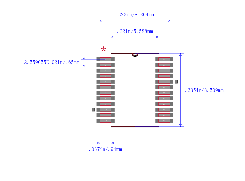
SN74ABT657ADBR
具有奇偶校验发生器/校验器和三态输出的八路收发器 24-SSOP -40 to 85
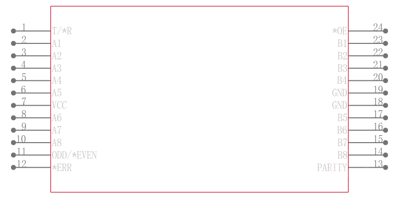
The "ABT657A transceivers have eight noninverting buffers with parity-generator/ checker circuits and control signals. The transmit/receive T/R\\\\ input determines the direction of data flow. When T/R\ is high, data flows from the A port to the B port transmit mode; when T/R\ is low, data flows from the B port to the A port receive mode. When the output-enable OE\\\\ input is high, both the A and B ports are in the high-impedance state.
Odd or even parity is selected by a logic high or low level on the ODD/EVEN\ input. PARITY carries the parity-bit value; it is an output from the parity generator/checker in the transmit mode and an input to the parity generator/checker in the receive mode.
In the transmit mode, after the A bus is polled to determine the number of high bits, PARITY is set to the logic level that maintains the parity sense selected by the level at ODD/EVEN\\\\. For example, if ODD/EVEN\ is low even parity selected and there are five high bits on the A bus, PARITY is set to the logic high level so that an even number of the nine total bits eight A-bus bits plus parity bit are high.
In the receive mode, after the B bus is polled to determine the number of high bits, the error ERR\\\\ output logic level indicates whether or not the data to be received exhibits the correct parity sense. For example, if ODD/EVEN\ is high odd parity selected, PARITY is high, and there are three high bits on the B bus, ERR\ is low, indicating a parity error.
When VCC is between 0 and 2.1 V, the device is in the high-impedance state during power up or power down. However, to ensure the high-impedance state above 2.1 V, OE\ should be tied to VCC through a pullup resistor; the minimum value of the resistor is determined by the current-sinking capability of the driver.
The SN54ABT657A is characterized for operation over the full military temperature range of -55°C to 125°C. The SN74ABT657A is characterized for operation from -40°C to 85°C.