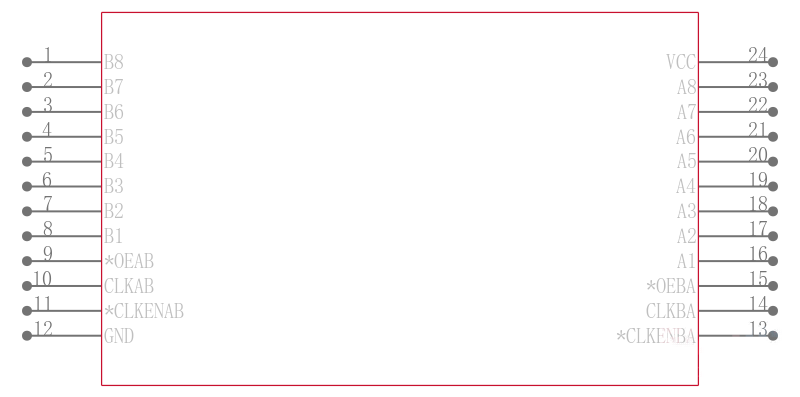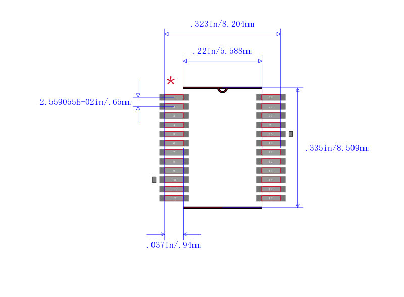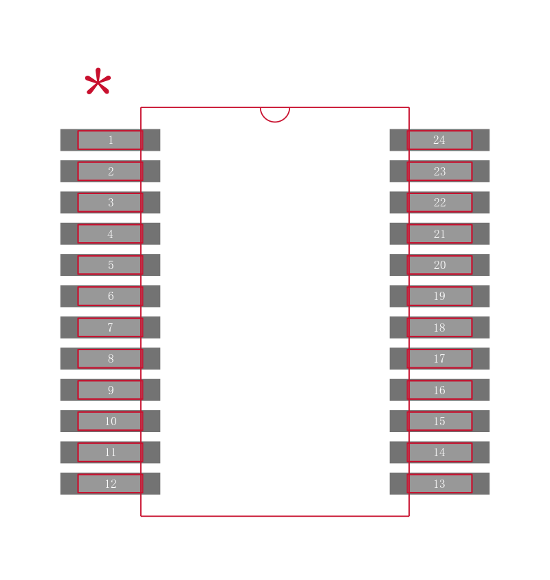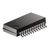
SN74LVC2952ADBR
八路总线收发器和具备三态输出寄存器 OCTAL BUS TRANSCEIVER AND REGISTER WITH 3-STATE OUTPUTS
This octal bus transceiver and register is designed for 1.65-V to 3.6-V VCC operation.
The SN74LVC2952A consists of two 8-bit back-to-back registers that store data flowing in both directions between two bidirectional buses. Data on the A or B bus is stored in the registers on the low-to-high transition of the clock CLKAB or CLKBA input, provided that the clock-enable CLKENAB\ or CLKENBA\ input is low. Taking the output-enable OEAB\ or OEBA\ input low accesses the data on either port.
Inputs can be driven from either 3.3-V or 5-V devices. This feature allows the use of these devices as translators in a mixed 3.3-V/5-V system environment.
To ensure the high-impedance state during power up or power down, OE\ should be tied to VCC through a pullup resistor; the minimum value of the resistor is determined by the current-sinking capability of the driver.
This device is fully specified for partial-power-down applications using Ioff. The Ioff circuitry disables the outputs, preventing damaging current backflow through the device when it is powered down.