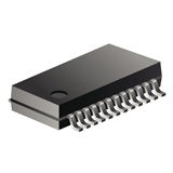
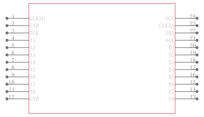
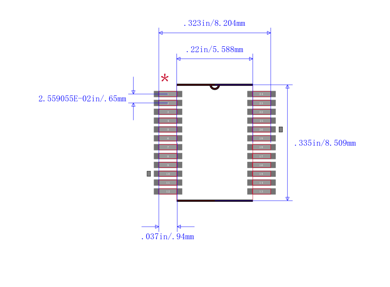
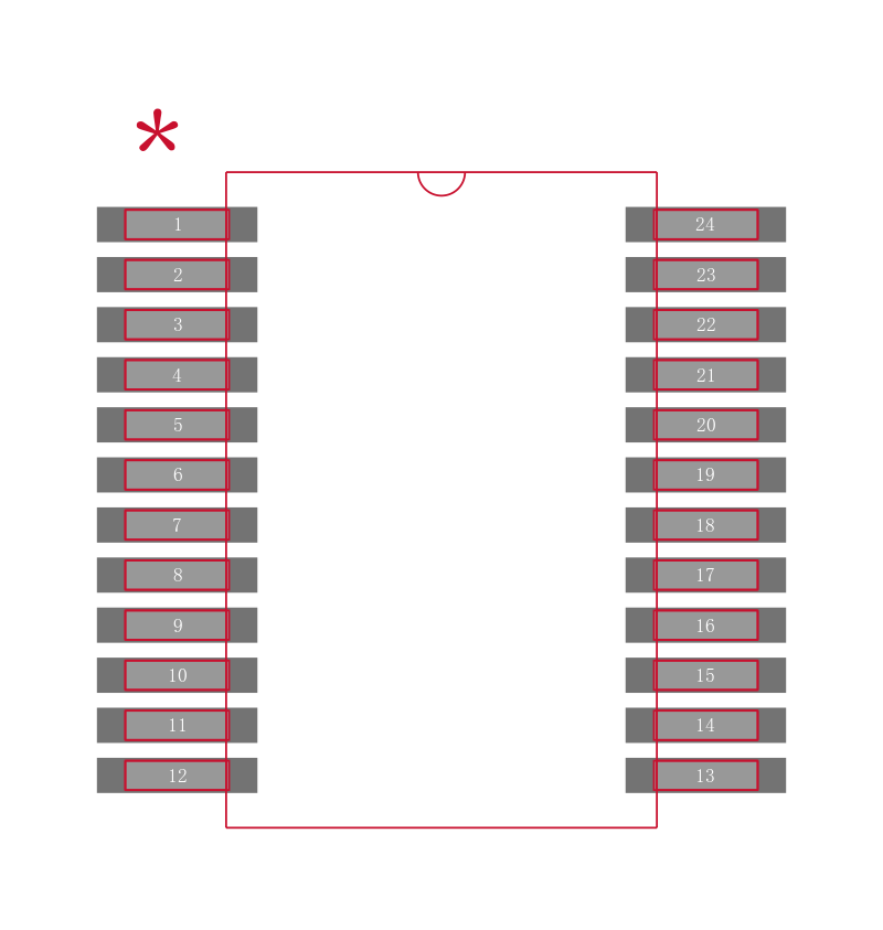
SN74ABT646ADBR
八路总线收发器和寄存器 OCTAL BUS TRANSCEIVERS AND REGISTERS
These devices consist of bus-transceiver circuits, D-type flip-flops, and control circuitry arranged for multiplexed transmission of data directly from the input bus or from the internal registers. Data on the A or B bus is clocked into the registers on the low-to-high transition of the appropriate clock CLKAB or CLKBA input. Figure 1 illustrates the four fundamental bus-management functions that can be performed with the ABT646A devices.
Output-enable OE\\\\ and direction-control DIR inputs are provided to control the transceiver functions. In the transceiver mode, data present at the high-impedance port can be stored in either register or in both.
The select-control SAB and SBA inputs can multiplex stored and real-time transparent mode data. The direction control DIR determines which bus receives data when OE\ is low. In the isolation mode OE\ high, A data can be stored in one register and/or B data can be stored in the other register.
When an output function is disabled, the input function still is enabled and can be used to store and transmit data. Only one of the two buses, A or B, can be driven at a time.
These devices are fully specified for partial-power-down applications using Ioff. The Ioff circuitry disables the outputs, preventing damaging current backflow through the devices when they are powered down.
To ensure the high-impedance state during power up or power down, OE\ should be tied to VCC through a pullup resistor; the minimum value of the resistor is determined by the current-sinking capability of the driver.


