MC100EPT21DTR2G
数据手册.pdfON SEMICONDUCTOR MC100EPT21DTR2G Voltage Level Translator, 2 Input, 1.4 ns, 3 V to 3.6 V, TSSOP-8 新
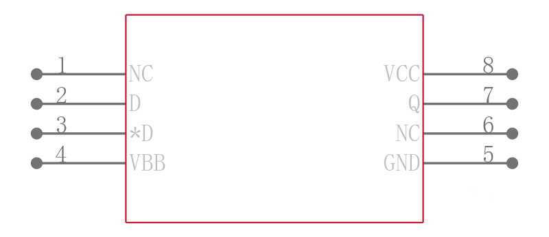
The is a 3.3V differential LVPECL/LVDS/CML to LVTTL/LVCMOS translator in 8 pin TSSOP package. Because LVPECL positive ECL, LVDS, positive CML input levels and LVTTL/LVCMOS output levels are used, only +3.3 V and ground are required. The small outline 8 lead SOIC package makes MC100EPT21DTR2G ideal for applications which require the translation of a clock or data signal. The VBB output allows this device to be cap coupled in either single ended or differential input mode. VBB output is tied to D input and D is driven for a non inverting buffer or VBB output is tied to the D input and D is driven for an inverting buffer when single ended cap coupled. VBB output is connected through a resistor to each input pin when cap coupled differentially. If used the VBB pin should be bypassed to VCC via a 0.01µF capacitor. It is used in precision clock translation applications.
- .
- 1.4ns typical propagation delay
- .
- Maximum frequency of 350MHz at TA = 25°C
- .
- LVPECL/LVDS/CML inputs, LVTTL/LVCMOS outputs
- .
- 24mA TTL outputs
- .
- Operating range VCC from 3V to 3.6V with GND = 0V
- .
- Temperature compensation and VBB output
- .
- Power supply current of 17mA outputs set to HIGH and 21mA outputs set to LOW
- .
- Duty cycle skew of 50% and part to part skew of 500ps at TA = 25°C
- .
- Output rise/fall times 0.8V to 2V of 600ps
- .
- Operating temperature range from -40°C to +85°C