MC74HC259ADTG
数据手册.pdfMC74HC259A: 8 位可寻址锁存 1/8 解码器
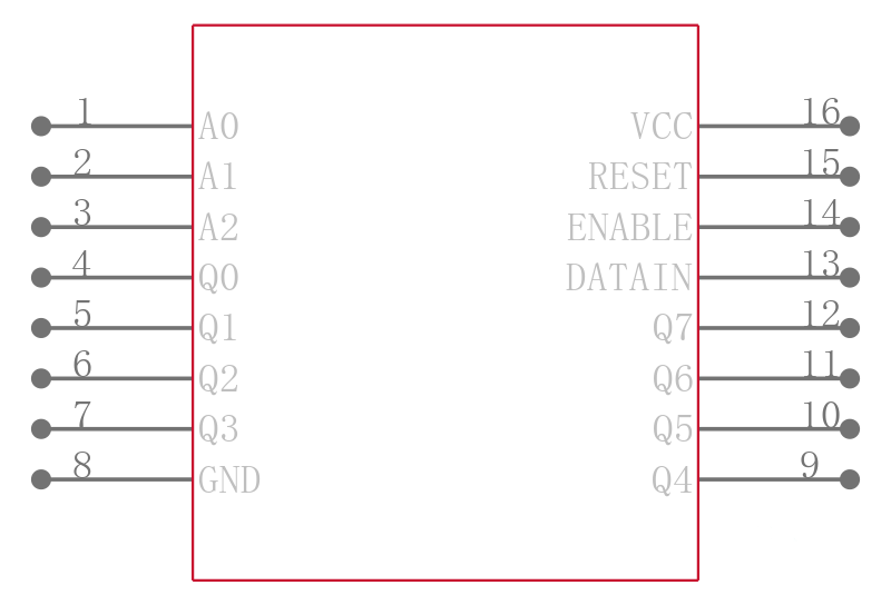
The MC74HC259A is identical in pinout to the LS259. The device inputs are compatible with standard CMOS outputs; with pullup resistors, they are compatible with LSTTL outputs. The HC259A has four modes of operation as shown in the mode selection table. In the addressable latch mode, the data on Data In is written into the addressed latch. The addressed latch follows the data input with all non addressed latches remaining in their previous states. In the memory mode, all latches remain in their previous state and are unaffected by the Data or Address inputs. In the one of eight decoding or demultiplexing mode, the addressed output follows the state of Data In with all other outputs in the LOW state. In the Reset mode all outputs are LOW and unaffected by the address and data inputs. When operating the HC259A as an addressable latch, changing more than one bit of the address could impose a transient wrong address. Therefore, this should only be done while in the memory mode.
Features
---
|
- .
- Output Drive Capability: 10 LSTTL Loads
- .
- Outputs Directly Interface to CMOS, NMOS, and TTL
- .
- Operating Voltage Range: 2 to 6 V
- .
- Low Input Current: 1 A
- .
- High Noise Immunity Characteristic of CMOS Devices
- .
- These are PbFree Devices